
Key Takeaways
- BOROFLOAT 33 offers high thermal shock resistance and low alkali content, making it ideal for anodic bonding and semiconductor processing.
- Alkali‑free glass wafers prevent ion migration that can damage sensitive electronics in display and MEMS applications.
- Surface quality and flatness specifications, such as scratch‑dig and wavefront error, are critical for optical and bonding performance.
- Custom sizes and coatings are available, with volume manufacturing options from prototype to mass production.
- All wafers comply with RoHS and REACH, with optional certifications for specific industries.
Why Glass Selection Defines Wafer Performance
When sourcing glass wafers for semiconductor packaging, MEMS, optical windows, or anodic bonding, the material and its coatings directly control yield, reliability, and optical throughput. A mismatched substrate can cause delamination, ion contamination, or poor transmission—failures that ripple into costly rework and field returns. This guide compares the most relevant glass types, with a focus on BOROFLOAT 33 and true alkali-free formulations, so your team can specify with confidence.

Candidate Glass Materials for Precision Wafers
Each glass category is suited to different thermal, electrical, and mechanical demands. The list below represents standard substrates used in wafer fabrication, including options that can be sourced as double-side polished, cut-to-size, or custom-diced blanks.
- Fused silica — Nearly pure SiO₂; offers extreme UV transmission, very low CTE (~0.55 × 10⁻⁶/K), and high softening point. Preferred for deep-UV optics and high-temperature photomasks, but comparatively expensive.
- Borosilicate (e.g., BOROFLOAT 33) — A floated low-alkali glass with a CTE of approximately 3.3 × 10⁻⁶/K. Its uniform flatness, minimal inclusions, and high transmission from near-UV to NIR make it a workhorse for anodic bonding to silicon and for MEMS cap wafers.
- Alkali-free glass (e.g., SCHOTT AF 32) — A true alkali‑free alumino‑borosilicate with CTE typically near 3.2 × 10⁻⁶/K. Eliminates mobile-ion contamination risk in semiconductor back-end and thin‑film transistor processes. Offers high strain point and excellent dielectric properties.
- Soda‑lime float glass — Economical, widely available, but high CTE (~9 × 10⁻⁶/K) and sodium content make it unsuitable for most semiconductor or high-temperature uses. May serve non‑critical protective cover applications.
- Aluminosilicate — Engineered for strength and scratch resistance; often chemically strengthened via ion exchange. Used where mechanical durability is paramount, such as cover glasses for displays or sensors.
- Sapphire (single‑crystal Al₂O₃) — Extreme hardness (9 Mohs), broad UV‑to‑mid‑IR transmission, and high thermal conductivity. Reserved for scratch‑proof windows, IR optics, and high‑stress environments where cost can be justified.
- Optical glass (e.g., N‑BK7, B270) — Tailored for visible‑range imaging and laser systems; offers tailored refractive index and dispersion but generally higher CTE and lower thermal resilience than borosilicates.
Key Properties and Honest Trade-Offs
The “boro 3.3” designation in BOROFLOAT 33 refers to its linear thermal expansion coefficient—roughly 3.3 µm/m·°C—which brings dimensional stability during thermal cycling and anodic bonding. Its alkali content is kept deliberately low, making it electrically insulating enough for many MEMS and microfluidic devices, though not as ion‑barrier as true alkali‑free glass. Alkali‑free wafers, by contrast, virtually eliminate ion migration; this becomes critical at elevated temperatures or in thin‑film‑transistor gate dielectrics.
Optical transmission is another differentiator: fused silica excels down to ~185 nm, while BOROFLOAT 33 transmits well from ~350 nm to 2 µm. Sapphire extends the range further into the mid‑IR. Hardness and chemical durability follow an inverse pattern—soda‑lime scratches easily but is cheap; sapphire resists almost everything but demands diamond tooling. Cost generally tracks purity and processing difficulty: fused silica and sapphire at the high end, soda‑lime at the low end, with borosilicate and alkali‑free glasses offering balanced performance‑per‑dollar.
Coating and Surface‑Treatment Options
Bare glass rarely meets end‑use specifications. The right coating turns a translucent substrate into a functional component:
- Anti‑reflection (AR) coatings — Multilayer dielectric stacks suppress reflection losses across a specified waveband. Essential for laser optics, camera windows, and any path where stray reflections degrade signal quality. Trade‑off: added cost and narrow acceptance angle.
- Mirror coatings (protected Al, Ag, Au) — Convert a wafer into a high‑reflectivity surface for scanning mirrors, retroreflective sensors, or decorative elements. Environmental durability varies with metal choice; Au excels in IR and resists tarnish.
- ITO (indium tin oxide) — Transparent conductive film for EMI/RFI shielding, defogging heaters, or capacitive touch surfaces. Sheet resistance and transparency must be balanced; typically adds 1–3% absorption in the visible.
- Hydrophobic/oleophobic layers — Fluoropolymer or silane monolayers that repel water and oils, easing cleaning and preventing contamination on sensor windows or medical device covers. Not a substitute for hermetic sealing.
- Thermal tempering / chemical strengthening — Tempering builds compressive surface stress through controlled heat treatment; chemical strengthening exchanges small ions (e.g., Na⁺ for K⁺) to create a deeper compressive layer. Both improve impact resistance but can introduce slight optical wavefront distortion—critical for aluminosilicate cover glasses.
Application Matching and Basic Compliance
For anodic bonding to silicon, BOROFLOAT 33 remains a widely trusted reference because its CTE matches silicon over the typical 300–450 °C bonding range, and its alkali content is low enough to avoid surface degradation. Where even trace sodium could compromise gate-oxide integrity, an alkali‑free wafer such as AF 32 is the safer choice, albeit at a higher unit cost.
High‑temperature process carriers or furnace windows favor fused silica, while IR sensor domes demand sapphire or CVD‑coated substrates. Display cover‑glass uses chemically strengthened aluminosilicate for its high compressive stress and impact resistance. Optical instrumentation often specifies B270 or N‑BK7 with broadband AR coatings.
On the regulatory side, all standard wafer glasses are RoHS and REACH compliant when handled without additional hazardous coatings. Electro‑plated metallic films or older coating processes may introduce substances of concern; our team verifies compliance per material batch before shipment.
Get a Material Recommendation for Your Project
Selecting the optimal glass and coating combination depends on wavelength range, thermal profile, mechanical load, and cost targets. Our applications engineers can review your requirements and propose a wafer stack that balances performance and budget. Reach out to start a material consultation.
Sourcing BOROFLOAT 33 and Alkali-Free Wafers: What to Specify
When sourcing borofloat 33 glass or alkali free glass wafers, buyers should specify material grade, dimensions, surface quality, and any required coatings. Tight tolerances on thickness (±0.02 mm) and diameter (±0.1 mm) are typical, while custom values can be dialed in for bonding or lithographic stacks. Surface flatness—often referenced by wavefront error (λ/4, λ/10 at 632.8 nm)—directly affects bonding uniformity and optical path length. Scratch-dig specifications per ISO 10110 or MIL-PRF-13830B (commonly 40-20 or better) control cosmetic defects that could compromise film adhesion or imaging contrast.
Key Specifications Checklist
- Material grade: SCHOTT BOROFLOAT 33, Corning alkali-free, or Chinese alkali‑free borosilicate
- Diameter: 50 mm–300 mm standard; custom sizes on request
- Thickness: 0.3 mm–2.0 mm with ±0.02 mm tolerance
- Flatness: λ/4 or λ/10 wavefront error at 632.8 nm
- Surface quality: 40-20 scratch-dig per ISO 10110, down to 10-5 achievable
- Edge finish: ground, polished, or chamfered to avoid chipping during handling
- Coatings: AR, ITO, or hydrophobic options applied after final cleaning
Quality and Compliance in Glass Wafer Production
All wafers are manufactured under ISO 9001‑certified processes to ensure lot‑to‑lot consistency. Each batch undergoes interferometric flatness measurement, profilometry for surface roughness (Ra < 1 nm typical for polished surfaces), and visual inspection per ANSI/OEOSC OP1.002. Material traceability is maintained from raw glass through final packaging, with certificates of conformance provided on request. Standard wafer glasses are RoHS and REACH compliant, and alkali‑free variants inherently avoid the ion migration risks that can degrade thin‑film transistor performance in display backplanes.
Customization and Volume Supply
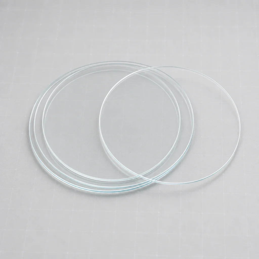
Both prototyping and volume production are supported, with standard 4 inch Borofloat 33 wafers available from stock for evaluation. Custom diameters, non‑circular shapes, and thicknesses outside the typical range are manufactured to order. Lead times scale with quantity and surface finish requirements, but samples can be shipped within weeks. All products are packaged in single‑wafer containers or vacuum‑sealed cassettes to prevent contamination and breakage during transit.
| Aspect | BOROFLOAT 33 | Alkali‑Free Glass |
|---|---|---|
| Base Composition | Borosilicate, low alkali | Boroa luminosilicate, virtually no alkalis |
| CTE (0–300 °C) | ≈ 3.25 × 10⁻⁶ /K | ≈ 3.0 × 10⁻⁶ /K |
| Thermal Resistance | Continuous use up to 450 °C | Moderate, typically up to 600 °C for short durations |
| Chemical Resistance | Excellent acid/alkali resistance | Very good, optimized for process chemicals |
| Transmission Range | 350 nm – 2.5 µm | Visible to near‑IR, over 90 % internal |
| Key Applications | Anodic bonding, MEMS, microfluidics | Display substrates, OLED, thin‑film electronics |
To discuss your requirements for BOROFLOAT 33 or alkali‑free glass wafers, contact our engineering team with your drawings or specifications. We provide feasibility feedback and a project‑specific quotation within 48 hours.
Frequently Asked Questions
What is Borofloat 33 glass?
Borofloat 33 is a floated borosilicate glass produced by SCHOTT. It has low alkali content, excellent thermal shock resistance (up to 450 °C continuous use), and high chemical durability. Its coefficient of thermal expansion closely matches silicon, making it the standard for anodic bonding in MEMS and wafer‑level packaging.
Is borofloat glass suitable for anodic bonding?
Yes, Borofloat 33 is widely used for anodic bonding to silicon because its CTE (≈3.25×10⁻⁶/K) is almost identical to that of silicon. The low alkali content ensures minimal ion movement during the electrostatic bonding process, yielding strong, hermetic seals for sensor and actuator devices.
What is the difference between Borofloat and standard borosilicate?
Borofloat is a specific brand of borosilicate glass manufactured by SCHOTT using a float process, resulting in exceptional flatness and uniform thickness. Standard borosilicate glass (e.g., Pyrex type) may have higher alkali content and slightly different thermal properties, making it less suitable for precision semiconductor applications.
What are alkali‑free glass wafers used for?
Alkali‑free glass wafers are used where even trace amounts of mobile alkali ions (Na⁺, K⁺) can degrade electronic performance—for example, in thin‑film transistor (TFT) backplanes for LCDs and OLEDs, touch panels, and organic electronics. They maintain high resistivity and stability during high‑temperature processing.
How should I specify surface quality on glass wafers?
Surface quality is typically specified using scratch‑dig numbers per ISO 10110 or MIL‑PRF‑13830B, such as 40‑20 or 10‑5. The first number is the maximum scratch width in microns, the second the maximum dig diameter in hundredths of a millimeter. Tighter specs reduce light scattering and improve bonding uniformity.