
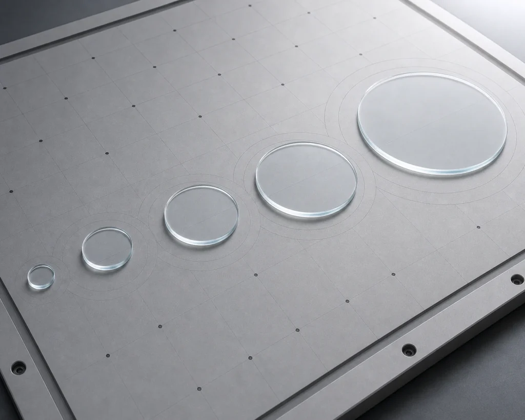
Key Takeaways
- Fused silica wafers provide exceptional UV transmission, low thermal expansion, and high laser damage resistance for precision optics.
- UV-grade (JGS1) and general-purpose (JGS2) fused silica grades meet different application requirements with distinct transmission and impurity profiles.
- Surface quality standards like MIL-PRF-13830 and flatness of λ/4 at 633 nm are typical specifications for optical-grade wafers.
- A fully controlled process—from material melting through double-side polishing, coating, and cleanroom packaging—ensures consistent batch-to-batch quality.
- B2B buyers should specify material grade, surface quality, edge finish, coatings, and acceptable TTV to receive accurate quotations.
Meeting the Demand for High-Performance Optical Substrates
Engineers and sourcing teams specifying materials for UV lithography, precision imaging, or laser systems face a strict set of requirements. The substrate must combine outstanding optical transmission from the deep-ultraviolet to the near-infrared, near-zero thermal expansion, and surface quality measured in angstroms. Fused silica wafers consistently meet these demands, making them a cornerstone of advanced optical manufacturing. Understanding how these wafers are produced—from raw material selection to final inspection—helps buyers evaluate supplier capabilities and ensure consistent quality in high-volume orders.

Base Materials and Inputs for Fused Silica Wafers
The performance of a fused silica wafer begins with the purity and type of silica feedstock. Two primary routes exist: synthetic silica, produced via chemical vapor deposition of high-purity silicon compounds, and natural quartz, melted from carefully selected crystalline quartz. Synthetic grades, often designated JGS1, offer the highest UV transmission below 250 nm and exceptionally low OH content, making them ideal for excimer laser applications. JGS2, derived from natural quartz, provides excellent visible and near-IR transmission at a more economical price point, while JGS3 delivers strong IR performance. While other optical glasses such as borosilicate or soda-lime may suffice for less demanding visible-spectrum tasks, and sapphire offers superior hardness, fused silica’s unique combination of wide-band transparency, low coefficient of thermal expansion (CTE), and high chemical purity sets it apart for critical optical components.
Step-by-Step Manufacturing Stages
Cutting and Scribing
Production begins with bulk fused silica ingots or blanks. Precision saws or laser scribing systems cut these into disc-shaped substrates close to the target diameter, minimizing material loss and edge chipping. The initial blank is intentionally oversize to accommodate subsequent material removal.
Grinding
Fine-grit diamond wheels bring the wafer to near-final thickness while establishing basic parallelism. Multi-spindle grinders can process both faces sequentially or simultaneously to control wedge and bow.
Lapping
A classic loose-abrasive lapping process with progressively finer alumina or diamond slurries removes the subsurface damage introduced by grinding. This stage achieves micron-level flatness and prepares the surface for polishing.
Polishing
High-precision double-side polishing is the critical step for optical wafers. Both faces are worked simultaneously between rotating plates with a chemical-mechanical polish (CMP) slurry, typically colloidal silica. This yields transmission-grade surfaces with roughness below 0.5 nm Ra and exceptional thickness uniformity across 100 mm to 300 mm diameters.
Edging and CNC Profiling
Final diameter is achieved via CNC edge grinding, creating a precise cylindrical profile or adding flats and notches as specified by SEMI or custom standards. This step also removes edge micro-cracks that could propagate under stress.
Drilling and CNC Machining
Ultrasonic or laser-assisted CNC drilling creates through-holes, counterbores, and complex features required for microfluidic devices, wafer carriers, or optical mounts—all while preserving the surrounding polished surface.
Coating
To enhance spectral performance, wafers may receive anti-reflective, high-reflective, or filter coatings. Magnetron sputtering and ion-assisted deposition guarantee dense, uniform layers with precise thickness control across the full face. Multilayer coatings are common for narrowband laser optics or broadband anti-reflection.
Strengthening (Optional)
Although fused silica is inherently robust and chemically resistant, additional thermal anneals or ion-exchange processes can further increase surface strength for high-stress environments or thin-substrate handling. This step is application-dependent and must not compromise optical quality.
Cleaning
The final stage is a multi-step cleaning sequence in an ISO Class 5 (or better) cleanroom. Ultrasonic or megasonic surfactant baths, followed by ultra-pure water rinsing and spin drying, eliminate particulate and organic residues without leaving water marks. Cleanliness is verified before packaging in certified containers.
Equipment and Techniques That Drive Quality
The precision of fused silica wafer manufacturing rests on advanced capital equipment. Double-side polishing machines with active plate temperature control enable the flatness and parallelism required for photomask blanks and wafer-level optics. CNC machining centers with diamond tooling produce edge profiles and features with micron-level tolerances. For coating, magnetron sputtering systems provide uniform deposition across large substrates, essential for consistent spectral performance. Finally, production within cleanroom environments—typically ISO Class 5 or 6—prevents contamination at every critical stage, from final polishing through inspection and packaging. These investments in equipment and process control directly correlate with the surface quality, dimensional accuracy, and lot-to-lot consistency that B2B buyers rely on.
In-Line Quality Checkpoints and Bulk-Order Consistency
At multiple points—after polishing, after coating, and before shipping—operators perform optical profilometry and interferometry to verify surface roughness, flatness, and transmitted wavefront error. Automated vision systems scan for scratch/dig defects per MIL-PRF-13830 or ISO 10110 standards. Spectrophotometric testing confirms transmission and reflectance against agreed-upon specifications. For bulk orders, statistical process control (SPC) tracks every parameter across production lots; data from these checkpoints demonstrate the manufacturer’s ability to deliver thousands of wafers with uniform optical and dimensional properties, which is critical for assembly lines and instrument OEMs.
Request a Factory Process Overview
Evaluating a potential fused silica wafer supplier goes beyond a datasheet. We encourage you to ask for a comprehensive process overview, including details on material sourcing, machine capabilities, cleanroom class, and in-line quality data. Such documentation helps you verify that the production environment matches the sophistication your application demands.
Fused Silica Wafers for Precision Optical Components
Fused silica wafers serve as the substrate of choice for precision optical components where high UV transmission, low coefficient of thermal expansion (CTE), and excellent laser damage resistance are non-negotiable. Typical applications include photomasks for lithography, beam splitter optics in high-power laser systems, and substrates for interference filters in medical devices. Unlike soda-lime or borosilicate glasses, fused silica wafers maintain dimensional stability across wide temperature swings, making them ideal for aerospace sensors and semiconductor metrology tools. Their transmission from deep UV through near-IR, combined with low autofluorescence, also suits them for biophotonic and spectroscopy platforms.
Key Facts for Sourcing Managers
- Fused silica wafers are available in UV-grade (JGS1) and general-purpose (JGS2) formulations, each offering distinct transmission curves and impurity levels.
- Standard diameters range from 50 mm to 300 mm, with thicknesses typically 0.5 mm to 2 mm, though larger and thinner custom dimensions can be achieved.
- Double-sided polishing to a 10-5 scratch-dig surface quality per MIL-PRF-13830 is common for optical-grade wafers.
- Total thickness variation (TTV) is typically controlled to ≤ 2 µm across a 100 mm wafer, essential for uniform optical path length.
- A wafer’s front and back surface flatness often meets λ/4 at 633 nm, enabling diffraction-limited optical assemblies.
- Anti-reflection (AR) coatings can be applied to both sides using ion-beam sputtering to reach R ≤ 0.5% per surface at designated wavelengths.
Attributes and Tolerances: What to Specify
When requesting a quotation, B2B buyers should clearly communicate the following parameters. For material, choose between JGS1 (high UV transmission, typical ≥ 90% at 185 nm) or JGS2 (cost-effective for visible/NIR use). For surface quality, refer to scratch-dig standards to balance cost and performance. Edge finish can be as-ground for handling safety, or etched to eliminate subsurface damage. Coatings—such as broadband AR, V-coat, or protective barrier layers—are specified by wavelength range and environmental durability requirements. Lead times and minimum order quantities (MOQ) depend on diameter, lot size, and secondary operations; expect rapid prototyping for standard sizes and longer lead times for tight TTV targets. Certifications like ISO 9001:2015 and material test reports traceable to the melt batch are typically available.
Certifications and Quality Standards
Leading fused silica wafer manufacturers adhere to ISO 9001 quality management systems and often maintain Class 100 (ISO 5) cleanrooms for final cleaning and packaging. In-process inspection uses automated interferometry for flatness, spectrophotometers for transmission, and optical microscopy for surface defects. Some suppliers provide in-house fused silica dicing data to guarantee die strength and edge chipping metrics. For semiconductor-lithography applications, trace metal analysis via ICP-MS may be offered to confirm contamination levels below 1 ppb for critical elements.
Process Overview at a Glance
| Stage | Key Equipment / Technique | Quality Control Parameter |
|---|---|---|
| Material Selection | Melt type (JGS1 vs JGS2), purity analysis | Transmission at 185 nm, OH content |
| Cutting/Scribing | CNC saw, laser scribing | Edge chipping, dimensional tolerance |
| Grinding & Lapping | Single- or double-side lapping machines | Thickness uniformity, TTV |
| Polishing | Double-side polishing, pitch/tin laps | Surface flatness (λ/4), Scratch/Dig |
| Edging & Drilling | CNC grinding centers, ultrasonic drilling | Diameter tolerance, hole position accuracy |
| Coating | Magnetron sputtering, IAD, ALD | Reflectance per surface, durability tests |
| Final Cleaning | Ultrasonic clean, Class 100 cleanroom | Particle count, visual inspection |
Request a Quote for Your Fused Silica Wafer Project
Whether you need a prototype fused silica wafer for a new optical instrument or a recurring supply of precision substrates for laser manufacturing, start a conversation with our engineering team. Provide your drawings or a detailed specification sheet, and we will prepare a competitive quote that includes all secondary operations, coatings, and packaging requirements.
Frequently Asked Questions
What is a fused silica wafer?
A fused silica wafer is a thin, flat disc made from high-purity synthetic or natural quartz glass (SiO₂) with ≥99.995% purity, known for its optical clarity and thermal stability. It is produced by melting ultrapure quartz and then slicing, grinding, lapping, and polishing to precise dimensions and surface finishes.
Is fused quartz the same as fused silica?
While often used interchangeably, fused silica typically refers to synthetic SiO₂ with high purity and low OH content for deep UV transmission, whereas fused quartz is derived from natural quartz crystal and may contain trace impurities. Both offer similar thermal and mechanical properties but fused silica is preferred for demanding UV and laser applications.
What are JGS1 and JGS2 grades in fused silica wafers?
JGS1 is a UV-grade synthetic fused silica with high transmission down to 185 nm and low impurity levels, ideal for lithography and UV optics. JGS2 is a general-purpose grade with good transmission in the visible and near-IR, often used where UV performance is not critical and cost is a factor.
What surface quality can be achieved on fused silica wafers?
Optical-grade fused silica wafers typically achieve 10-5 scratch-dig per MIL-PRF-13830 after double-side polishing, with surface flatness of λ/4 at 633 nm or better. More demanding applications can specify 20-10 or even 10-5 on both faces.
How do fused silica wafers compare to silicon wafers?
Fused silica wafers transmit light across a broad spectrum (UV to IR), whereas silicon wafers are opaque and used for semiconductor or MEMS devices. Fused silica offers superior thermal shock resistance and lower electrical conductivity, making it suitable for optical windows, substrates, and biosensors.