
Key Takeaways
- Borosilicate glass wafers, especially BOROFLOAT 33, provide the thermal and chemical stability required for long-lasting appliance sensors.
- With a CTE matching silicon, these wafers enable reliable anodic bonding for MEMS‑based pressure and flow sensors.
- Double‑side polished surfaces and optional AR coatings optimize optical transmission from UV to near‑IR.
- Standard wafer diameters range from 100 mm to 200 mm, with tight thickness and flatness tolerances maintained through precision lapping and polishing.
- Low minimum order quantities and cleanroom packaging support both prototyping and high‑volume production.
Meeting Sensor Reliability Goals Inside Demanding Appliances
Whether designing a pressure transducer for a washing machine, a turbidity sensor for a dishwasher, or a touch interface for an oven control panel, sensor components must perform predictably for years despite thermal cycling, humidity, chemical exposure, and mechanical vibration. The glass substrate or protective window at the heart of such a sensor needs to combine optical clarity, thermal stability, and chemical robustness without degrading signal integrity. A borosilicate glass wafer is often the most practical starting point, offering a balanced combination of properties that appliance manufacturers trust.
How Borosilicate Glass Wafers Address the Core Challenges
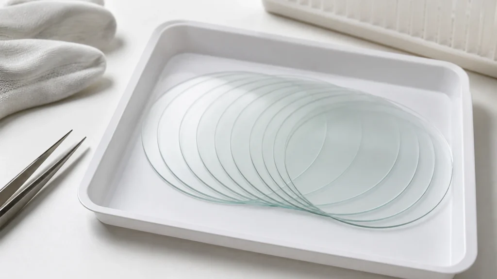
Borosilicate glasses — with Borofloat 33 glass being a widely specified float-glass example — deliver a low coefficient of thermal expansion (CTE approximately 3.3 × 10⁻⁶/K), high transmission from the visible into the near-infrared, and strong resistance to water, acids, and alkaline cleaning agents. Available as precision appliance sensor wafers in standard diameters (100 mm, 150 mm, 200 mm) and thicknesses down to a few hundred microns, these substrates serve as stable platforms for thin‑film sensor structures, anodic bonding to silicon, or durable optical windows. Their surface flatness typically meets single‑digit micron total thickness variation (TTV) requirements, enabling consistent lithography and reliable hermetic sealing.
Key Selection Criteria for Sensor Substrates
Choosing the right glass wafer for an appliance sensor application involves evaluating several interrelated material and processing parameters:
- Transmission and spectral range. For optical sensors, verify the internal transmittance at the operating wavelengths; borosilicate excels from 350 nm to 2 µm, which covers many LED and photodetector combinations.
- Thermal expansion match. To avoid stress during temperature changes, the CTE should align with bonded materials such as silicon. Borosilicate’s low expansion minimizes warpage and seal failure in thermal cycling tests.
- Flatness and surface quality. MEMS‑based pressure or flow sensors demand tight TTV and low roughness; the float process inherently yields fire‑polished surfaces, but custom lapping and polishing can refine flatness further.
- Durability under appliance conditions. Resistance to humidity, detergent solutions, and thermal shock is essential. Borosilicate meets hydrolytic class 1 requirements and withstands repeated exposure to boiling water and steam.
- Regulatory compliance. Confirm RoHS and REACH compliance for the European market, and check for any food‑contact safety requirements if the sensor sits near consumables.
From Prototype to Production: A Typical Development Journey
Consider a team developing a compact turbidity sensor for a next‑generation dishwasher. Early prototypes use 4‑inch borofloat 33 glass wafers with an anti‑reflection coating on one side and a hydrophobic layer on the other to prevent fogging. After verifying optical performance and surviving a 1000‑hour life test in hot detergent, the design moves to pilot production. The wafer supplier provides statistically controlled batches with documented TTV and wedge, ensuring that the dispensing equipment bonds each die consistently. As volumes ramp, the supplier transitions to custom‑cut rectangular substrates sawn from larger wafers, maintaining the same material pedigree and quality records. This scaled approach keeps the BOM predictable and the supply chain transparent.
Planning Ahead: Tolerances, Coatings, and Logistics
Sensor designers should lock in specifications early to avoid revalidation. Critical items to discuss with your glass supplier include:
- Dimensional tolerance stack‑up. Wafer thickness, wedge, and diameter tolerances directly affect the sensor’s optical path length or cavity depth. Tighten them where necessary but allow standard tolerances where possible to control cost.
- Coating compatibility. If the wafer requires anti‑reflective, conductive, or anti‑fingerprint coatings, ensure the glass surface finish and cleaning protocol are compatible. The supplier may offer in‑house coating services or recommend qualified partners.
- Integration and packaging. Plan for die singulation methods, cleaning before bonding, and handling procedures that avoid edge chipping. Anodic bonding compatibility assumes alkali mobility in the glass—a property intrinsic to borosilicate.
- Logistics and traceability. For high‑volume appliance programs, wafer carriers and cleanroom packaging prevent particulate contamination, and lot‑level traceability supports recall readiness.
Discuss Your Sensor Substrate Requirements
Every appliance sensor project brings a unique set of demands. Whether you need optical-grade windows for a smart washer or thermally stable substrates for an industrial pressure transmitter, our technical team can help translate your performance targets into a practical glass wafer specification. Reach out to start a conversation about your current design challenges.
Borosilicate Glass Wafers Provide Unmatched Reliability for Appliance Sensor Components
Borosilicate glass wafers form the foundation of reliable appliance sensors by maintaining dimensional stability under thermal cycling and resisting chemical attack from household cleaning agents. Their high transmission from UV to near-IR enables accurate optical sensing in washing machines, dryers, refrigerators, and smart home devices. Often specified as SCHOTT BOROFLOAT® 33, this material complies with ISO 3585 (type 3.3) standards and delivers the combination of low alkali content and high flatness required for anodic bonding to silicon—a common method for integrating pressure and flow sensors.
When you select borosilicate glass wafers, you are investing in a substrate proven to survive millions of appliance cycles without performance drift. The amorphous structure eliminates grain boundaries that could initiate cracks, while the borosilicate network provides a thermal expansion coefficient closely matched to silicon, reducing interfacial stress in bonded stacks.
Key Specifications That Influence Sensor Performance
Key Facts about Borosilicate Glass Wafers for Sensors
- Made from SCHOTT BOROFLOAT® 33 or equivalent, compliant with ISO 3585 type 3.3 borosilicate glass.
- Coefficient of thermal expansion (CTE) of approximately 3.25 × 10⁻⁶ K⁻¹ (20–300°C), enabling stress-free anodic bonding to silicon.
- High visible and near-infrared transmission, typically >90% from 350 nm to 2000 nm, with negligible autofluorescence.
- Resists thermal shock up to 450°C and withstands most household chemicals, including detergents and mild acids.
- Available in standard wafer diameters from 100 mm to 200 mm, with surface roughness down to <1 nm Ra after polishing.
Material and Thermal Properties
The cornerstone of appliance sensor reliability is thermal stability. Borosilicate glass wafers, especially those fabricated from SCHOTT borofloat 33 glass, exhibit a low CTE that prevents warpage during temperature swings from –40°C to 450°C. This is critical for sensors inside ovens, water heaters, and outdoor smart meters. The hydrolytic resistance (Class 1 per ISO 719) ensures long-term clarity even in high-humidity environments, and the material’s acid and alkali durability protects against aggressive cleaning solutions.
Optical and Surface Quality
For optical sensors that rely on transmission, borosilicate wafers offer high transparency from the UV through the near-infrared. Double-side polishing achieves surface flatness of ≤2 µm total thickness variation (TTV) and roughness below 1 nm Ra, minimizing scatter and insertion loss. Optional anti-reflective (AR) coatings can be applied in-house or through qualified partners, further boosting signal-to-noise ratios in spectrophotometric and fluorescence-based detectors used in premium appliances.
Ordering and Logistics Considerations
Sensor-grade borosilicate wafers are typically supplied in diameters ranging from 100 mm to 200 mm, with thicknesses from 0.5 mm to 2.0 mm. Custom dimensions, edge profiling, and precision coring are available to match your sensor array layout. Minimum order quantities (MOQs) are flexible, supporting both pilot builds and volume ramp-ups. Standard lead times for common diameters are short; custom processing may require additional planning. All wafers are shipped in cleanroom-grade wafer carriers with lot-level traceability for ISO 9001 and RoHS compliance.
Summary of Borosilicate Glass Wafer Attributes for Appliance Sensor Applications
| Attribute | Typical Value / Range | Impact on Sensor Performance |
|---|---|---|
| Material Grade | SCHOTT BOROFLOAT® 33 or equivalent ISO 3585 type 3.3 borosilicate | Ensures thermal and chemical compliance |
| CTE (20–300°C) | ~3.25 × 10⁻⁶ K⁻¹ | Matches silicon, enabling stress-free anodic bonding |
| Transmission Range | >90% from 350 nm to 2000 nm | High signal throughput for optical sensors |
| Surface Roughness (Ra) | <1 nm after double-side polishing | Minimizes scatter and improves bonding |
| Wafer Diameters | 100 mm, 150 mm, 200 mm standard | Compatible with standard MEMS and sensor fabrication lines |
| Thermal Shock Resistance | Up to 450°C sustained | Withstands dishwasher and dryer environments |
| Chemical Durability | Hydrolytic class 1, acid and alkali resistant | Resists cleaning agents and condensation |
Start Your Sensor Substrate Qualification
Every appliance sensor project has unique optical, mechanical, and environmental requirements. Our applications engineers can help translate your performance targets into a glass wafer bonding or window specification that marries form, fit, and long-term reliability. Submit your drawings or reach out to discuss a feasibility review—together we can shorten your path from prototype to production.
Frequently Asked Questions
Why is borosilicate glass preferred for appliance sensor components?
Its low coefficient of thermal expansion prevents stress during temperature swings, and its high chemical resistance withstands exposure to detergents and humidity. Additionally, it offers excellent optical clarity for sensor windows.
What is the difference between BOROFLOAT 33 and generic borosilicate glass?
BOROFLOAT 33 is a trademarked floated borosilicate glass from SCHOTT with exceptionally high flatness and surface quality, meeting ISO 3585 type 3.3 standards. It provides higher visible transmission and better thermal shock resistance than many common borosilicate glasses.
Can borosilicate glass wafers be anodically bonded to silicon?
Yes, borosilicate glass contains mobile alkali ions (primarily sodium) that enable anodic bonding to silicon at elevated temperatures and voltages. This creates a hermetic seal essential for MEMS pressure and flow sensors in appliances.
What surface finishes are available for sensor-grade borosilicate wafers?
Typical finishes include double-side polished with surface roughness below 1 nm Ra. Optional anti-reflective (AR) coatings can be applied to maximize transmission in the sensor's operating wavelength range.
What quality certifications do borosilicate glass wafer suppliers typically provide?
Reputable suppliers offer material certificates confirming compliance with ISO 3585, along with lot-specific data on transmission, CTE, and flatness. Full RoHS and REACH declarations are standard, and cleanroom processing with particle counts down to Class 100 is common.