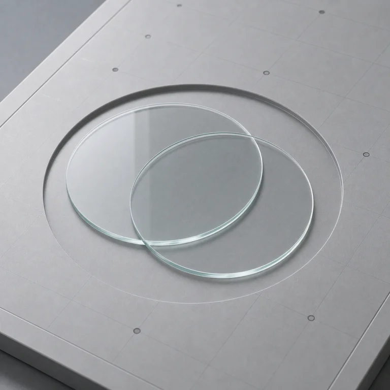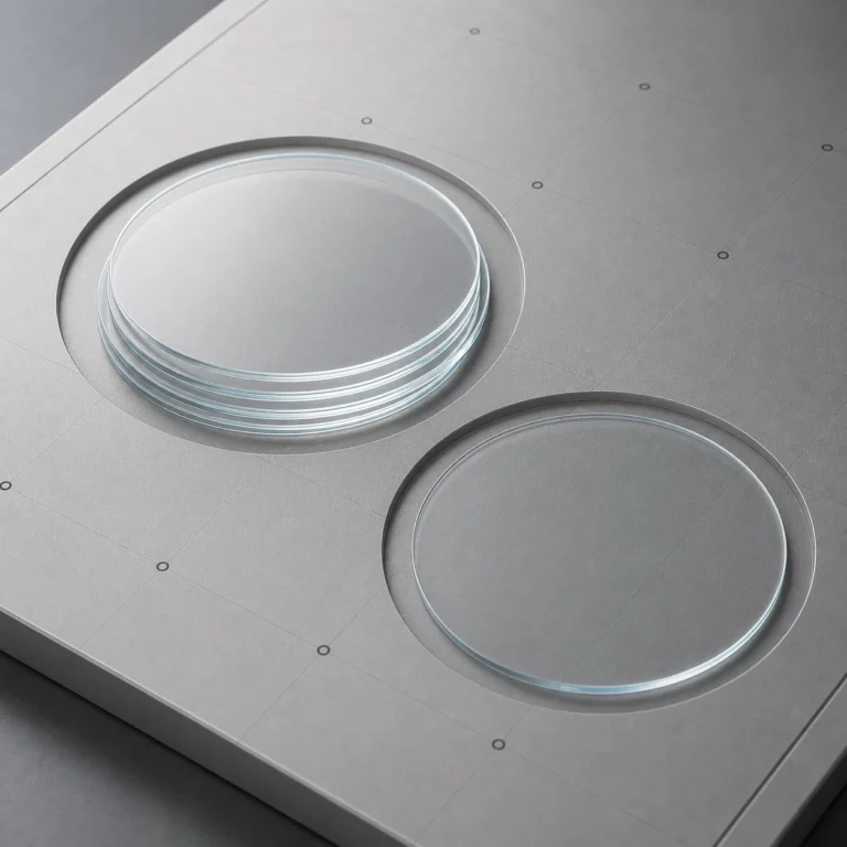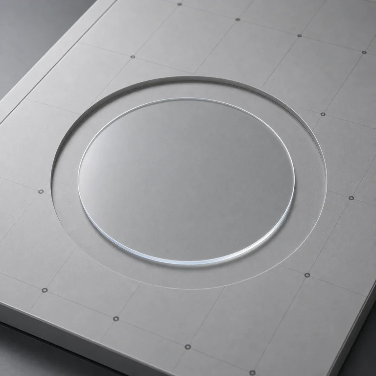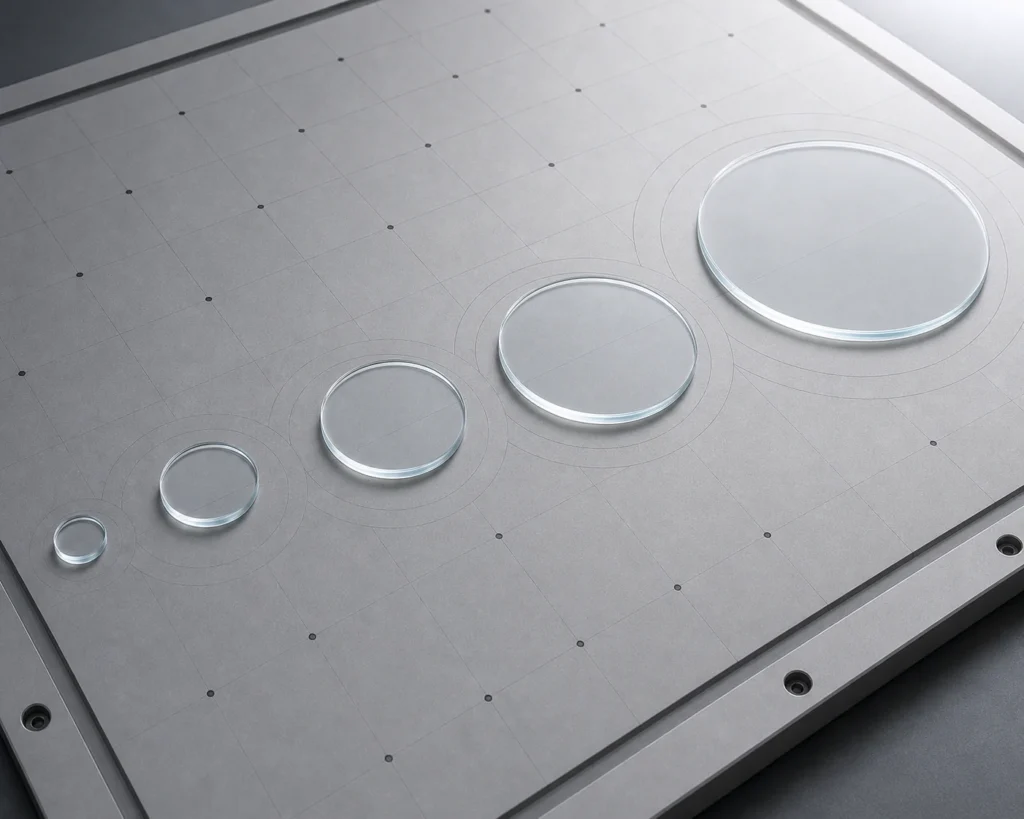
UV and optical grade fused silica wafers, laser-marked and cleanroom packed. Every glass & quartz wafers part is made to your drawing, so dimensions, material grade, coatings and finish are all specified by you and verified in-house before shipping.
Overview
Fused Silica Glass Wafers (2–12", JGS1/JGS2) is produced from Fused silica, quartz and borosilicate wafers from 2 to 12 inches, diced, ground and cleaned for semiconductor and photonics processing. We machine, finish and inspect the part under one roof, which keeps tolerances, surface quality and documentation consistent from prototype through to production quantities.
Typical applications
Customers use this component across photonics, semiconductor, biomedical and instrumentation work. Whether it goes into an optical path, a sensor stack, a diagnostic device or a piece of process tooling, the geometry and surface specification can be tuned to your exact requirement.
How we make it
Depending on the design we combine femtosecond laser ablation, CNC ultrasonic machining, precision dicing, optical polishing, thin-film coating and thermal or anodic bonding. A design-for-manufacturing review checks feasibility before cutting, so problems are caught on the drawing rather than on the shop floor.
Specifications
| Grade | JGS1 / JGS2 |
|---|---|
| Diameter | 2–12 inch |
| Thickness | 0.3–3.0 mm |
| TTV | ≤ 5 µm |
Request a quote
Send a STEP, DXF or PDF drawing with your tolerances, material and quantity and we will respond with feasibility and lead time. You can also configure this part in the 3D Glass Builder and submit the specification directly.