
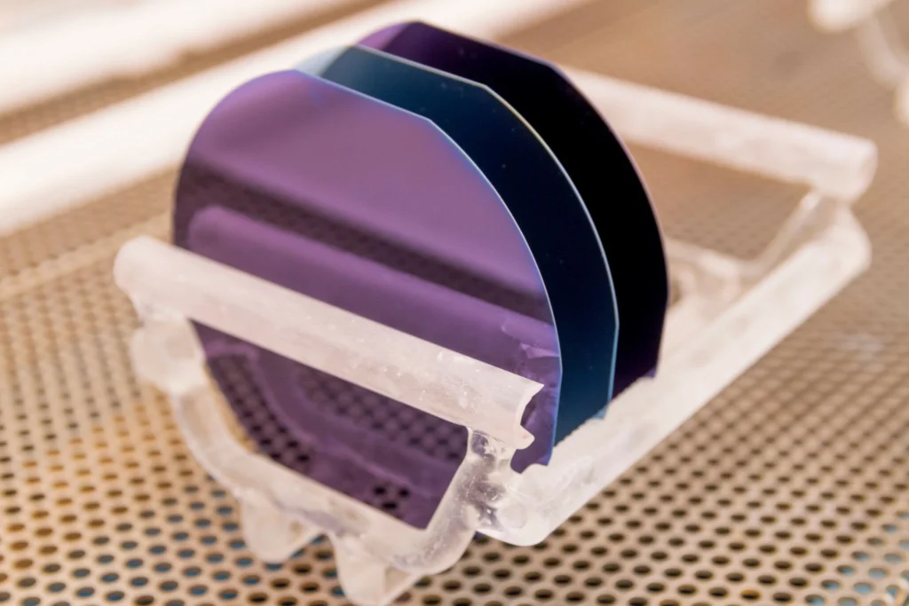
Fused Silica Glass Wafers for MEMS: Fused Silica (CTE 0.55 x 10^-6 /K, 185 nm – 2.5 um). Single-piece prototypes to production volumes, quoted from your drawing.
fused silica glass wafers for mems programs need anodic-bondable wafers with tight TTV. Fused Silica is the fit here because it offers near-zero thermal expansion. Typical parts: cap wafers, TGV substrates, motion-sensor lids.
Specifications at a glance
| Material | Fused Silica (JGS1 (UV), JGS2 (standard), JGS3 (IR)) |
|---|---|
| Thermal expansion (CTE) | 0.55 x 10^-6 /K |
| Service temperature | 1,100 C continuous |
| Transmission range | 185 nm – 2.5 um |
| Density | 2.20 g/cm3 |
| Knoop hardness | 500 kg/mm2 |
| Refractive index | 1.458 @ 587 nm |
| Stock thickness | 0.10 – 50 mm |
| Maximum blank size | 450 x 450 mm |
| Wafer formats | 2", 3", 4", 6", 8" and 12" with SEMI flats or notch |
| TTV | under 3 – 5 um by format |
| RFQ inputs | PDF/DXF/STEP drawing, quantity brackets, surface and edge spec |
Capabilities and limits
One material, many routes: on Fused Silica we also quote sandblasting, laser cutting, drilling, polishing, and multi-step drawings are the norm rather than the exception.
DFM notes from the shop floor
Three items decide most of the cost and lead time on this work:
- Material note: its hardness and brittleness demand diamond tooling and controlled feeds.
- Over-specification is the quiet budget killer: a 20/10 scratch-dig face costs roughly three times an 80/50 face, so grade each surface individually.
The full rules live in our tolerance design guide and holes and edges design guide.
Typical applications
The recurring buyers of fused silica glass wafers for mems: laboratory instruments (cuvettes, sight glasses, stir-cell windows); aerospace optics (sensor windows, star-tracker flats, radiation-tolerant ports); ccd inspection equipment (CCD cover plates, reference grids, stage glass). Background reading on the underlying material science: RP Photonics: fused silica.
The fastest route to a quote is geometry: use the 3D builder below, draw a dimensioned 2D drawing from it, or open the site-wide custom glass machining 3D + 2D builder for fully custom parts.
Related reading on this site: glass hole micromachining, CNC machining capability, CCD screening plates.
Frequently asked questions
Is there a minimum order for fused silica glass wafers for mems?
No. Single prototypes are accepted, and pricing steps down at 10, 100 and 1,000 pieces.
How fast can prototypes ship?
Machined prototypes ship in 5 – 10 working days. Coated or bonded parts add 1 – 2 weeks depending on queue slots.
What files do you need for a quote?
A dimensioned PDF plus DXF or STEP geometry. If only a sketch exists, our drawing review service formalizes it before quoting.
Do parts ship with inspection data?
Dimensional reports, surface certificates and material certs per melt are available; specify the level on the RFQ.
What tolerances are achievable on Fused Silica parts?
Ground features hold +/-0.01 mm and lapped thickness reaches +/-0.003 mm. Its hardness and brittleness demand diamond tooling and controlled feeds.
Specifications on this page were last reviewed by our engineering team in September 2026.