
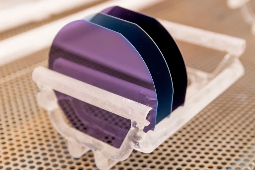
Fused Silica Glass Wafers for MEMS: Fused Silica (CTE 0.55 x 10^-6 /K, 185 nm – 2.5 um). Single-piece prototypes to production volumes, quoted from your drawing.
fused silica glass wafers for mems programs need anodic-bondable wafers with tight TTV. Fused Silica is the fit here because it offers near-zero thermal expansion. Typical parts: cap wafers, TGV substrates, motion-sensor lids.
Specifications at a glance
| Material | Fused Silica (JGS1 (UV), JGS2 (standard), JGS3 (IR)) |
|---|---|
| Thermal expansion (CTE) | 0.55 x 10^-6 /K |
| Service temperature | 1,100 C continuous |
| Transmission range | 185 nm – 2.5 um |
| Density | 2.20 g/cm3 |
| Knoop hardness | 500 kg/mm2 |
| Refractive index | 1.458 @ 587 nm |
| Stock thickness | 0.10 – 50 mm |
| Maximum blank size | 450 x 450 mm |
| Wafer formats | 2", 3", 4", 6", 8" and 12" with SEMI flats or notch |
| TTV | under 3 – 5 um by format |
| RFQ inputs | PDF/DXF/STEP drawing, quantity brackets, surface and edge spec |
Manufacturing capability
One material, many routes: on Fused Silica we also quote etching, lapping, drilling, grinding, and multi-step drawings are the norm rather than the exception.
Design guidance
Before sending the RFQ, check these against your drawing:
- Material note: its hardness and brittleness demand diamond tooling and controlled feeds.
- Over-specification is the quiet budget killer: a 20/10 scratch-dig face costs roughly three times an 80/50 face, so grade each surface individually.
The full rules live in our tolerance design guide and holes and edges design guide.
Application context
The recurring buyers of fused silica glass wafers for mems: microfluidic devices (chips, manifolds, via plates, bonded stacks); medical diagnostics (flow cells, slides, microplate bottoms, cuvette windows); optical sensors (sensor windows, filter caps, lens covers). Background reading on the underlying material science: RP Photonics: fused silica.
The fastest route to a quote is geometry: use the 3D builder below, draw a dimensioned 2D drawing from it, or open the site-wide custom glass machining 3D + 2D builder for fully custom parts.
Engineers scoping this work usually also review wafer dicing process, fused silica material guide, tolerance design guide.
Frequently asked questions
What files do you need for a quote?
A dimensioned PDF plus DXF or STEP geometry. If only a sketch exists, our drawing review service formalizes it before quoting.
Do parts ship with inspection data?
Dimensional reports, surface certificates and material certs per melt are available; specify the level on the RFQ.
What tolerances are achievable on Fused Silica parts?
Ground features hold +/-0.01 mm and lapped thickness reaches +/-0.003 mm. Its hardness and brittleness demand diamond tooling and controlled feeds.
What thickness range do you stock for Fused Silica?
Standard stock spans 0.10 – 50 mm, with blanks up to 450 x 450 mm. Other formats are sourced per order.
How does Fused Silica behave under heat?
CTE is 0.55 x 10^-6 /K and continuous service reaches 1,100 C continuous, which is what drives its use where near-zero thermal expansion matters.
Specifications on this page were last reviewed by our engineering team in October 2026.