
Multi-Die Chips Gain Reach and Efficiency from Optical Integration
Data centre operators and high-performance computing architects are confronting a hard physical limit: the electrical interconnects that shuttle bits between chiplets inside advanced packages can no longer keep pace with throughput demands without imposing crippling power and thermal penalties. Co-packaged optics, or CPO, is now moving from a lab curiosity to a practical design choice because it directly confronts those penalties. By replacing long electrical traces with photonic links right at the package substrate, CPO slashes interconnect power, extends the distance between active compute dies, and allows designers to pack far more bandwidth onto a single package than copper alone can deliver.
Breaking the Copper Bottleneck
Multi-die architectures such as chiplets promise enormous economic and performance gains by letting foundries mix process nodes and reuse proven IP blocks. The promise hits a wall, however, when those tightly spaced silicon tiles must communicate across an organic interposer or a silicon bridge. Copper traces suffer from sharply rising resistive losses and cross-talk as data rates climb above 100 Gbps per lane, forcing equalization and retiming circuits that consume precious on-chip power and area.

Optical connections sidestep the problem entirely. A modulated laser beam passing through a waveguide experiences negligible attenuation over the centimetre distances relevant to a package, effectively removing the frequency-dependent loss that haunts electrical channels. Design teams that adopt CPO report that they can retire bulky driver chains and complex signal-conditioning macros, reclaiming both energy and floorplan space for compute logic.
Leading-edge foundries and packaging houses already offer initial CPO-enabled platforms. TSMC’s COUPE (Compact Universal Photonic Engine) integrates a silicon photonics interposer beneath compute chiplets, while Intel has demonstrated optical chiplets within its EMIB bridge technology. These implementations show that photonics can carry aggregate bandwidths of multiple terabits per second across a standard organic substrate without resorting to exotic cooling.
Energy Efficiency and Reach Advantages
Perhaps the most immediate operational payoff is a steep drop in picojoules per bit. Early CPO demonstrators have shown interconnect energy below 0.5 pJ/bit, compared with 5–10 pJ/bit for an equivalent electrical link that includes SerDes and forward error correction. Over hundreds of lanes, the saving translates to tens of watts removed from the package power budget, which directly improves the thermal design envelope of every server, switch, or accelerator card that uses the technology.
Reach benefits matter just as much at the system level. While copper can reliably drive signals only a few centimetres at high speed, photonic interconnects can stretch across an entire printed circuit board or even span shelves inside a rack. This decouples the placement of high-power logic dies from memory stacks and networking ASICs, giving system architects liberty to optimise cooling and power delivery without being forced to cluster hot components.
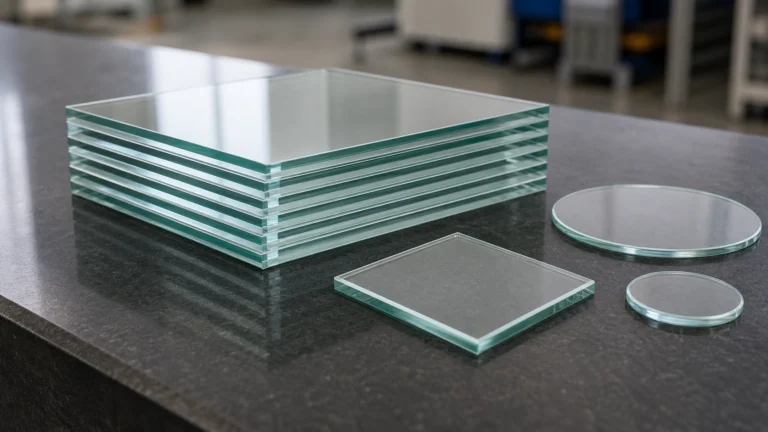
Thin glass materials are now being evaluated as optical waveguide carriers precisely because they combine the necessary transparency, thermal stability, and large-area processing economics. Quartz glass sheets and Borofloat 33 wafers are gaining attention as candidate substrates for planar lightwave circuits embedded in advanced packages, offering low optical loss and compatibility with standard wafer-scale manufacturing steps.
Bandwidth Density for Next-Gen Workloads
Artificial-intelligence training clusters and disaggregated memory pools require east–west bandwidth densities that are already exceeding what copper planes can deliver inside a single rack. CPO changes the arithmetic by allowing hundreds of wavelength-division-multiplexed channels to be routed through a single fibre array attached to the package edge. This offers a capacity roadmap that scales with laser modulation speed and wavelength count, not with the geometric limits of copper traces.
Standardisation efforts are solidifying around the UCIe (Universal Chiplet Interconnect Express) specification, which now includes a streaming protocol that is compatible with optical physical layers. Coupling UCIe with optical engines means a chiplet designer can map native die-to-die traffic directly onto photonic lanes, avoiding the protocol-conversion overhead that has historically limited the practicality of optical links inside a package.
System vendors are eyeing CPO not just for niche supercomputers but for volume cloud infrastructure. A single CPO-enabled switch ASIC mating 51.2 Tbps of switching bandwidth with optical engines at the package perimeter eliminates the need for pluggable optics and the corresponding faceplate complexity, simplifying both the bill of materials and the field-reliability profile.
Integration Challenges and Ecosystem Readiness
For all its promise, CPO demands a multi-physics assembly flow that is still maturing. Laser sources must be attached with sub-micron alignment and kept stable over a 10-year operational life while sitting next to logic dies that cycle through wide temperature swings. Foundries are tackling this with integrated micro-ring modulators and on-package monitoring photodiodes, but the test and burn-in infrastructure for photonic chiplets remains a work in progress.
The economic equation is shifting, however. The cost of a discrete pluggable optical module is falling slowly, while the per-bit energy cost of driving longer copper traces is rising with each datarate step. Analysts project that for aggregate bandwidths above 25 Tbps per package, the total system-level power saving from CPO alone will outweigh the incremental assembly cost, pulling the technology into mainstream switching and GPU interconnects.
Fabless companies and system integrators are now running active evaluations, and early adopter platforms are expected to enter volume production within the next two years. The focus is moving from feasibility demonstrations to qualifying reliability, yield, and supply-chain resilience for the laser arrays and photonic chips that form the heart of every CPO implementation.
| Aspect | Electrical (Copper) | Optical (CPO) | Operational Impact |
|---|---|---|---|
| Energy per bit | 5–10 pJ/bit | <0.5 pJ/bit (demonstrated) | Reduces package power by tens of watts |
| Reach | <10 cm at high speed | Meters across board/rack | Decouples logic and memory placement |
| Bandwidth density | Limited by trace geometry | Scales with wavelength and fibre count | Enables AI clusters and disaggregated memory |
| Signal conditioning | Complex SerDes, equalization | Minimal optical link design | Simplifies die floorplan |
| Maturity | Proven and reliable | Early adoption stage | Infrastructure and standards developing |
As silicon photonics manufacturing yields improve and the UCIe optical extension hardens, co-packaged optics will transition from a performance hero to an everyday design tool, reshaping how system architects partition and connect their multi-die silicon.
Why This Matters
Integrating optics directly into semiconductor packaging represents a fundamental shift from electrical to photonic interconnects, enabling the next generation of AI accelerators and high-performance switches to scale without hitting a power wall. As the industry standardises CPO interfaces, the technology will lower data-centre energy consumption and unlock denser, more flexible system architectures.
FAQ
What are co-packaged optics?
Co-packaged optics place optical transceivers directly on the same substrate as compute or switch ASICs, using photonic waveguides instead of long electrical traces to carry data between dies. This approach eliminates the energy-hungry electrical serializer/deserializer interfaces and front-panel pluggable modules, integrating the conversion from electrical to optical signals inside the package.
How does CPO benefit multi-die chip designs?
Multi-die designs mix and match chiplets on a single package, but the dense electrical wiring between them becomes a bottleneck at high bandwidths. CPO delivers low-loss, high-bandwidth optical links that can span centimetres to metres without the power and thermal overhead of advanced electrical equalization, enabling designers to place compute, memory, and I/O tiles more freely and scale aggregate throughput well beyond what copper can support.
Which companies are leading CPO development?
Major semiconductor foundries and chip makers are actively developing CPO platforms. TSMC has its COUPE silicon photonics interposer, Intel is combining optical chiplets with its EMIB bridge technology, and networking companies such as Broadcom and Cisco are integrating CPO into switch ASICs to eliminate pluggable modules. A broader ecosystem of optical component suppliers and packaging houses is forming to support volume production.
When will co-packaged optics become mainstream?
Initial CPO-enabled products are already appearing in high-end network switches and are expected to enter wider adoption over the next two to three years. Volume deployment for AI accelerators and disaggregated memory systems is projected once the supply chain for laser arrays and photonic chiplets reaches mature yields, likely by the mid-to-late 2020s.
Sources
Source: Semiconductor Engineering