
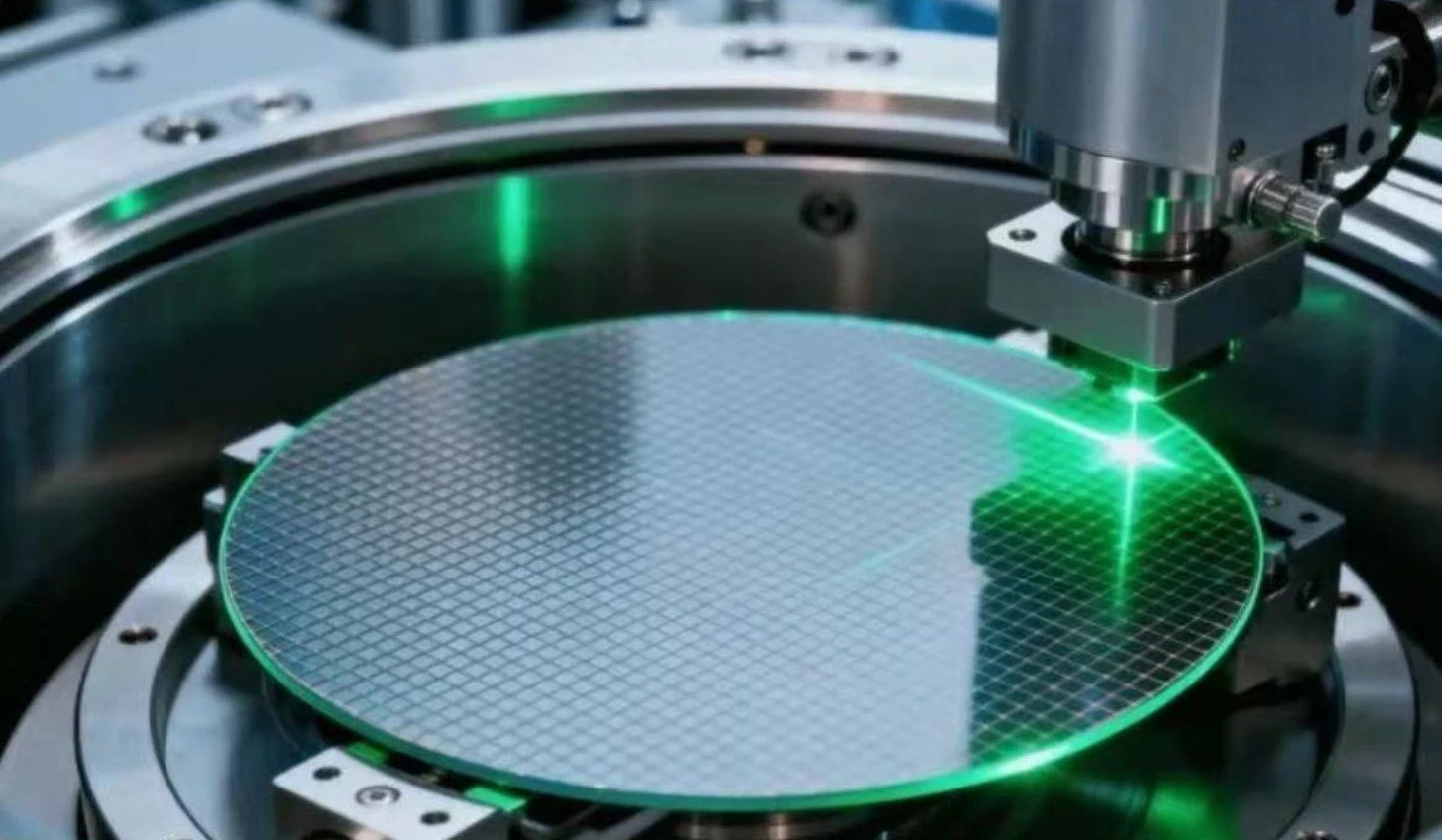
Application: Rubber, Plastic, Chemical, Ceramic, Glass. Model: Photolithography.
Overview
The Glass-Based Photolithography Biochip for Automated Droplet Generation Factory is supplied as a glass microfluidic chip made from Silicon Dioxide,Sin,. It is used in Rubber, Plastic, Chemical, Ceramic and Glass. Dimensions, material grade, coating and finish can be quoted to your drawing; the values above are the listed starting point.
Specifications
| Material | Silicon Dioxide,Sin, |
|---|---|
| Application | Rubber, Plastic, Chemical, Ceramic, Glass |
| Model NO. | Photolithography |
| Model | Customized |
| Breadth Depth Ratio | Customized |
| Accuracy | 6inch |
| ISO 13485 | 2016 |
| Supplier | Zhejiang Zegota Precision Technology Co., Ltd. |
Technical data
| Capability Item | Description / International Standard Specs |
|---|---|
| Primary Technology | High-Resolution Stepper Photolithography, Laser Direct Writing, Silicon DRIE, Glass/Quartz Wet Etching |
| Chip Substrates | Silicon-based, Quartz-based, Soda-lime Glass, Borosilicate Glass, and SU-8/PDMS/COP polymers |
| Exposure Resolution (CD) | ≤ 350mm (Sub-micron features, ultra-fine electrode pitches, micropillar arrays) |
| Overlay Alignment Accuracy | ≤ 100mm (For complex multi-mask, multi-layer microfluidic structures) |
| Etching Aspect Ratio | Up to 20:1 (Silicon DRIE); Etching depth uniformity variation ≤± 2% |
| Surface Modification | Hydrophilic/Hydrophobic tuning, PEGylation, Silanization, Biotin-Streptavidin coating |
| Cleanroom Standard | Class 10/100 Photolithography Yellow Rooms, GMP Class 10,000 packaging |
| Quality Management | ISO 13485:2016 (Medical Devices Quality), FDA Registered, CE Compliant |
| Foundry Service Model | Mask Design→ Photo-masking →Lithography & Etching → Dicing → Surface Functionalization → Assembly |
What to specify when you request a quote
- Material — listed as “Silicon Dioxide,Sin,”; name the glass or quartz grade.
- Outline and thickness — give outline, thickness and tolerances.
- Holes, slots and features — dimension every hole and its position tolerance on the drawing.
- Edges — state edge finish and chamfer.
- Surface — state polish and flatness where they matter.
Engineering guides for this part
For material grades and coating options, see BF33 Glass for Microfluidic Chips: Properties, Coatings & Selection Guide. How parts like this are machined and finished is covered in Glass Wafer Bonding for Microfluidic and MEMS Applications: Process Overview. For an application example, read Custom Glass Microfluidic Chips for Appliance Fluid Detection. A related standard product is Custom Glass Microfluidic Chip.


