
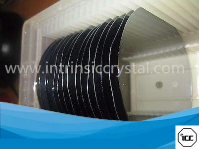
Product type: Round. Application: Optical. Model: D5~D300.
Overview
The Optical Sapphire Silicon Quatz 1'~8" Wafer is supplied as a sapphire / specialty wafer made from Silicon Sapphire Quatz. Listed geometry: diameter 1", 2", 3", 4", size 1", 2", 3", 4", SAW grade and Optical grade., thickness 0.55 ± 0.05 mm, 0.45 ± 0.05 mm, or other size, single-lens shape. Optical / electrical data: transmittance >95%. Coating: UV. Typical applications: Optical. Dimensions, material grade, coating and finish can be quoted to your drawing; the values above are the listed starting point.
Specifications
| Material | Silicon Sapphire Quatz |
|---|---|
| Type | Round |
| Shape | Single-lens |
| Diameter | 1", 2", 3", 4" |
| Size | 1", 2", 3", 4", SAW grade and Optical grade. |
| Thickness | 0.55 ± 0.05 mm, 0.45 ± 0.05 mm, or other size |
| Transmittance | >95% |
| Coating | UV |
| Usage | Optical |
| Model NO. | D5~D300 |
| Lenses Color | Clear |
| N-type | P (Phosphorus), Sb(Antimony ), As (Arsenic) |
| P-type | B (Boron) |
| CZ | from 1mOhm.cm to 150 Ohm.cm |
| FZ | up to 10k Ohm.cm |
| On standard | (100)(110)(111) |
| On request | (211)(311)(411)(511)(711)(911)(210)(310)(510)(910)(531)(731) |
| Standard | +/-0.5 |
| On polished surface | < 1 nm |
| Growth method | hydro-thermal autoclave. Sigle crystal, no twinning allowed. |
| Bow | < 10 microns |
| TTV | < 10 um |
| Orientation | X cut, Z cut or other, tolerance: ± 0.25 degrees |
| Primary Flat Location | ± 0.10 degrees unless specified |
| Primary Flat Length | 2"-16mm, 3"-22mm, 4"-32mm |
| Surface Polish Quality | SAW grade mirror polish |
| Backside | Lapped with GC1100# (W14) |
| Secondary Flat | – One flat, 180 deg from the primary flat. |
| Supplier | Qinhuangdao Intrinsic Crystal Technology Co., Ltd. |
Technical data
| Diameter | 1" inch25.4mm | 2" inch50.8mm | 3"inch76.2mm | 4 "inch100mm | 5"inch125mm | 6"inch150mm | Other diameters per request |
| ThicknessStandard(um) | 250 | 275 | 380 | 525 | 625 | 675 | from 120 um to 15nn |
| TTV Std(um) | <10 | <10 | <10 | <10 | <10 | <10 | |
| TTV min SSP(um) | 5 | 5 | 5 | 5 | 10 | 10 | |
| TTV min DSP(um) | 3 | 3 | 3 | 3 | 3 | 3 | |
| BOW (um) | <30 | <30 | <30 | <30 | <30 | <30 | |
| Particle count | 10-25 | 10-25 | 10-25 | < 10 | < 15 | < 15 | |
| ThicknessTolerance(+/-um) | 15 | 25 | 25 | 20 | 20 | 20 | |
| Type&dopant | N-type: P (Phosphorus), Sb(Antimony ), As (Arsenic) | ||||||
| P-type: B (Boron) | |||||||
| undoped | |||||||
| Resistivity | CZ: from 1mOhm.cm to 150 Ohm.cm | ||||||
| FZ: up to 10k Ohm.cm | |||||||
| orientation | On standard: (100)(110)(111)On request: (211)(311)(411)(511)(711)(911)(210)(310)(510)(910)(531)(731) | ||||||
| Tolerance | Standard:+/-0.5o | On request: +/-0.05o | |||||
| Off orientation | Up to 40o | ||||||
| Surface | As cut, Lapped, Etched, Single side polished, Double side polished | ||||||
| Roughness | On polished surface : < 1 nm | ||||||
| Flatness | On polished surface : < 1 um |
| Range of diameter | Dia.0.7mm-Dia.400mm |
|---|---|
| Range of curve radius | R1.5-R∞ etc. |
| Tolerance of diameter | +/-0.1, +/-0.01, +/-0.005 etc. |
| Surface accuracy | λ , 1/2λ , 1/4λ , 1/10λ etc. |
| Tolerance of Thickness | +/-0.1, +/-0.05, +/-0.01 etc. |
| Centration | +/-2′,+/-1′ etc. |
| Aperture N | 5, 1 etc. |
| Irregularity ΔN | 2, 1, 0.5, 0.2 etc. |
| Surface quality | 60/40, 40/20, 20/10, 10/5 etc. |
| Standard Specifications | |
|---|---|
| Growth method | CZ |
| Crystal structure | Hexagonal |
| Orientation | C-plane off to M-Plane 0.2 degree , A-plane , R-plane , M-plane |
| Dielectric constant | 11.58 |
| Lattice constant | 4.77 A |
| Tolerance of orientation | +/- 0.5 ° |
| Size | 2" , 3" , 4" Other sizes available upon request |
| Thickness | 330 um(2") , 430 um(2", 3") , 0.5 mm(3", 4"), 0.65mm(4"), 0.8mm(4") |
| Surface finish | one side or two sides epi polished |
| Surface roughness | Ra <= 2 A |
| Package method | Single wafer container or Ampak cassette, 100 grade clean room |
What to specify when you request a quote
- Diameter and flat / notch — listed as “1", 2", 3", 4"”; state diameter, flat or notch and their tolerances.
- Thickness and TTV — listed as “0.55 ± 0.05 mm, 0.45 ± 0.05 mm, or other size”; give thickness, its tolerance and total thickness variation.
- Polish and roughness — listed as “< 1 nm”; specify single- or double-side polish and roughness.
- Flatness, bow and warp — listed as “< 10 microns”; quote flatness, bow and warp limits.
- Material grade — listed as “Silicon Sapphire Quatz”; name the grade (JGS1/JGS2, Borofloat 33, alkali-free, sapphire orientation).
Engineering guides for this part
For material grades and coating options, see Fused Quartz Wafer Substrate Selection: Materials & Coatings for Semiconductor and Optical Systems. How parts like this are machined and finished is covered in Precision Glass Hole Machining for MEMS and Wafer Parts.


