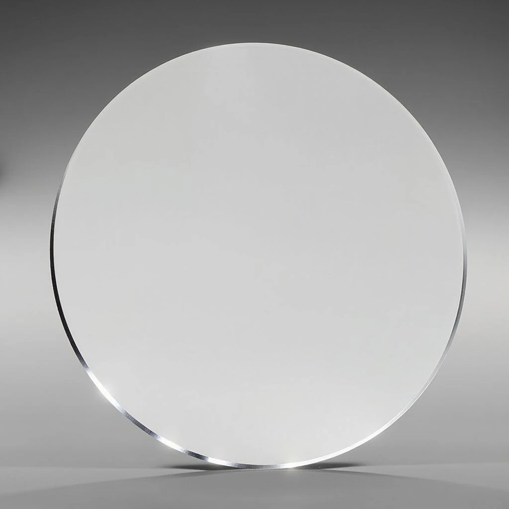
Model: 2INCH.
Overview
Sapphire Wafer 3inch R-Axis Al2O3 Sapphire Crystal Wafers is a sapphire / specialty wafer. Listed geometry: round shape. Dimensions, material grade, coating and finish can be quoted to your drawing; the values above are the listed starting point.
Specifications
| shape | Round |
|---|---|
| Conductive Type | Unipolar Integrated Circuit |
| Integration | ULSI |
| Technics | Thick Film IC |
| Model NO. | 2INCH |
| Keyword | LED Substrates |
| Products | LED Substrates Sapphire Wafer |
| a=4.758 Å,Å c=12.991 Å, c | a=2.730 |
| Supplier | Zhejiang Camp-Shinning New Material Co., Ltd. |
Technical data
| GENERAL | |||
| Chemical Formula | Al2O3 | ||
| Crystal Stucture | Hexagonal System ((hk o 1) | ||
| Unit Cell Dimension | a=4.758 Å,Å c=12.991 Å, c:a=2.730 | ||
| PHYSICAL | |||
| Metric | English (Imperial) | ||
| Density | 3.98 g/cc | 0.144 lb/in3 | |
| Hardness | 1525 – 2000 Knoop, 9 mhos | 3700° F | |
| Melting Point | 2310 K (2040° C) | ||
| STRUCTURAL | |||
| Tensile Strength | 275 MPa to 400 MPa | 40,000 to 58,000 psi | |
| at 20° | 400 MPa | 58,000 psi (design min.) | |
| at 500° C | 275 MPa | 40,000 psi (design min.) | |
| at 1000° C | 355 MPa | 52,000 psi (design min.) | |
| Flexural Stength | 480 MPa to 895 MPa | 70,000 to 130,000 psi | |
| Compression Strength | 2.0 GPa (ultimate) | 300,000 psi (ultimate) |
| Standard wafer 2 inch C-plane sapphire wafer SSP/DSP 3 inch C-plane sapphire wafer SSP/DSP 4 inch C-plane sapphire wafer SSP/DSP 6 inch C-plane sapphire wafer SSP/DSP | Special Cut A-plane (1120) sapphire wafer R-plane (1102) sapphire wafer M-plane (1010) sapphire wafer N-plane (1123) sapphire wafer C-axis with a 0.5°~ 4° offcut, toward A-axis or M-axis Other customized orientation |
|---|---|
| Customized Size 10*10mm sapphire wafer 20*20mm sapphire wafer Ultra thin (100um) sapphire wafer 8 inch sapphire wafer | Patterned Sapphire Substrate (PSS) 2 inch C-plane PSS 4 inch C-plane PSS |
| 2inch | DSP C-AXIS 0.1mm/ 0.175mm/0.2mm/0.3mm/0.4mm/0.5mm/1.0mmt SSP C-axis 0.2/0.43mm(DSP&SSP) A-axis/M-axis/R-axis 0.43mm |
|---|---|
| 3inch | DSP/ SSP C-axis 0.43mm/0.5mm |
| 4Inch | dsp c-axis 0.4mm/ 0.5mm/1.0mmssp c-axis 0.5mm/0.65mm/1.0mmt |
What to specify when you request a quote
- Diameter and flat / notch — state diameter, flat or notch and their tolerances.
- Thickness and TTV — give thickness, its tolerance and total thickness variation.
- Polish and roughness — specify single- or double-side polish and roughness.
- Flatness, bow and warp — quote flatness, bow and warp limits.
- Material grade — name the grade (JGS1/JGS2, Borofloat 33, alkali-free, sapphire orientation).
Engineering guides for this part
For material grades and coating options, see Fused Quartz Wafer Substrate Selection: Materials & Coatings for Semiconductor and Optical Systems. How parts like this are machined and finished is covered in Precision Glass Hole Machining for MEMS and Wafer Parts.
FAQ
What should I include in a quote request? expand_more
Include diameter and flat / notch, thickness and ttv, polish and roughness, flatness, bow and warp and material grade, plus quantity and a drawing if the part is custom.