
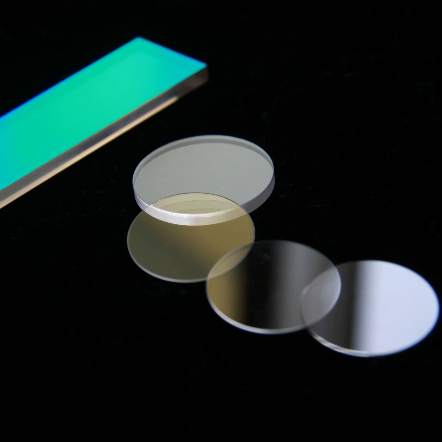
Product type: Flat Lens. Application: Lighting, Medical. Model: OC-0025.
Overview
Polished Sapphire Wafer Single Side 2-Polishing Fabrication Services is a sapphire / specialty wafer in Optical Glass (Monocrystalline Silicon substrate). Listed geometry: diameter 1mm – 500mm (standard sizes available, custom dimensions supported), single-lens shape. Optical / electrical data: transmittance >95%. Surface quality Polished to Ra ≤ 0.01μm, no scratches, bubbles, or impurities. Typical applications: Temperature Measurment & Optics Applying. Dimensions, material grade, coating and finish can be quoted to your drawing; the values above are the listed starting point.
Specifications
| Material | Optical Glass |
|---|---|
| Substrate | Monocrystalline Silicon |
| Type | Flat Lens |
| Shape | Single-lens |
| Transmittance | >95% |
| Surface Quality | Polished to Ra ≤ 0.01μm, no scratches, bubbles, or impurities |
| Parallelism | Less Than 1 Arc Min |
| Application | Temperature Measurment & Optics Applying |
| Usage | Lighting, Medical |
| Model NO. | OC-0025 |
| Lenses Color | Clear |
| Purity | Sog-Si |
| Conductivity Type | All |
| Size Tolerance | 0/-0.15mm |
| Thickness Tolerance | +/-0.05mm |
| Surface Finish | 60-40 Scratch-Dig |
| Manufacturing Technology | Optoelectronic Semiconductor |
| Excellent mechanical strength | Sapphire has extremely high hardness and strength, with a Mohs hardness of 9, which makes it perform well in various environments and resist scratches and wear. |
| Good thermal stability | Sapphire wafers can remain stable at high temperatures and are suitable for high temperature applications. |
| High transparency | Sapphire wafers have good transparency in the visible and ultraviolet ranges and are suitable for optical components and lasers. |
| Low thermal conductivity | Although sapphire has high thermal stability, its thermal conductivity is relatively low, which makes it very useful in some applications, such as as an insulating material. |
| Excellent chemical stability | Sapphire has good tolerance to many chemicals and is suitable for use in a variety of environments. |
| Semiconductor devices | Used to manufacture LEDs, laser diodes and other optoelectronic devices, sapphire wafers are an important substrate material for blue and white LEDs. |
| Optical devices | Due to its excellent transparency, sapphire wafers are widely used in optical windows, lenses and optical components. |
| High-temperature electronic devices | Sapphire wafers can be used to manufacture high-performance electronic devices under high temperature and harsh environments. |
| Sensors | Used to manufacture high-precision sensors and detectors, especially in applications that require high temperature resistance and corrosion resistance. |
| sizes | 2 inches, 4 inches, 6 inches, etc. |
| Diameter Range | 1mm – 500mm (standard sizes available, custom dimensions supported) |
| Optical Performance | High light transmittance (≥92% for visible light), low chromatic aberration, precise focal length |
| Tolerance | Dimensional tolerance ±0.02mm, focal length tolerance ±1% |
| Coating Option | Anti-reflective coating (AR coating), hydrophobic coating, or custom coating as per request |
| Supplier | C-Laser (Taicang) Material Technology Co., Ltd. |
Technical data
| Material | Sapphire (Al2O3) |
|---|---|
| Crystal Structure | Single crystal (Single Sapphire) |
| Diameter | Common sizes: 2 inches, 4 inches, 6 inches, etc. |
| Thickness | Typically 0.5 mm to 1.5 mm |
| Surface Roughness | Ra < 10 nm (can be finer as needed) |
| Defect Density | Less than 100 cm² |
| Thermal Conductivity | Approximately 25 W/m·K |
| Refractive Index | Approximately 1.76 |
| Chemical Stability | Acid and alkali resistant |
| Operating Temperature Range | High-temperature resistant, typically up to 1500°C |
What to specify when you request a quote
- Diameter and flat / notch — listed as “0/-0.15mm”; state diameter, flat or notch and their tolerances.
- Thickness and TTV — listed as “+/-0.05mm”; give thickness, its tolerance and total thickness variation.
- Polish and roughness — listed as “Polished to Ra ≤ 0.01μm, no scratches, bubbles, or impurities”; specify single- or double-side polish and roughness.
- Flatness, bow and warp — quote flatness, bow and warp limits.
- Material grade — listed as “Optical Glass”; name the grade (JGS1/JGS2, Borofloat 33, alkali-free, sapphire orientation).
Engineering guides for this part
For material grades and coating options, see Fused Quartz Wafer Substrate Selection: Materials & Coatings for Semiconductor and Optical Systems. How parts like this are machined and finished is covered in Precision Glass Hole Drilling & Micromachining for MEMS Wafers.


