
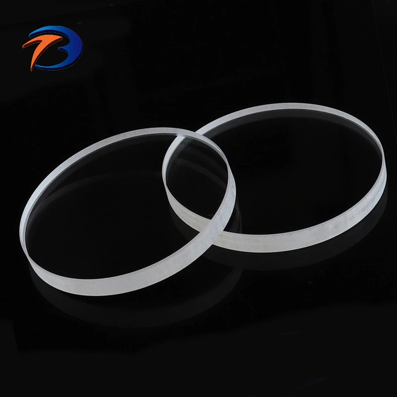
SKU MG-EC0DCF

Thin Diameter 15mm CaF2 Calcium Fluoride Optical Window Wafer Instrument

Thin Diameter 15mm CaF2 Calcium Fluoride Optical Window Wafer Instrument — a sapphire / specialty wafer: Optical Glass. Specs, RFQ checklist and custom…

Optical GlassMaterial
Optical WindowsType
FlatShape
>95%Transmittance
Thin Diameter 15mm CaF2 Calcium Fluoride Optical Window Wafer Instrument

Product type: Optical Windows. Application: Lighting, Medical, Optical, Photography.

Overview

Thin Diameter 15mm CaF2 Calcium Fluoride Optical Window Wafer Instrument: a sapphire / specialty wafer made from Optical Glass. Listed geometry: flat shape. Optical / electrical data: transmittance >95%. Typical applications: Lighting, Medical, Optical and Photography. Dimensions, material grade, coating and finish can be quoted to your drawing; the values above are the listed starting point.

Specifications

Material Optical Glass
Type Optical Windows
Shape Flat
Transmittance >95%
Usage Lighting, Medical, Optical, Photography
Lenses Color Clear
Supplier Shenyang Ebetter Optics Co., Ltd.

Technical data

Diameter 0.2-300mm
Thickness 0.1-100mm
Dimension tolerance +/-0.1mm or +/-0.02mm
Surface quality (scratch & dig) 60/40, 40/20 or better
Clear aperture >85%, >90%
Surface accuracy L/10 L/2 L
Parallelism +/-3' ,+/-30''
Bevel 0.1~0.3mm x 45 degree
Coating AR, BBAR or Custom

What to specify when you request a quote

  • Diameter and flat / notch — state diameter, flat or notch and their tolerances.
  • Thickness and TTV — give thickness, its tolerance and total thickness variation.
  • Polish and roughness — specify single- or double-side polish and roughness.
  • Flatness, bow and warp — quote flatness, bow and warp limits.
  • Material grade — listed as “Optical Glass”; name the grade (JGS1/JGS2, Borofloat 33, alkali-free, sapphire orientation).

Engineering guides for this part

For material grades and coating options, see Fused Quartz Wafer Substrate Selection: Materials & Coatings for Semiconductor and Optical Systems. How parts like this are machined and finished is covered in Glass Wafer Bonding for Microfluidic and MEMS Applications: Process Overview. For an application example, read Infrared Window Glass for Smart Home Appliance Sensors. Before sending a drawing, check Specifying Coatings for Custom Glass Windows and Substrates. A related standard product is Infrared Windows.

FAQ

What is the Thin Diameter 15mm CaF2 Calcium Fluoride Optical Window Wafer Instrument made of? expand_more
It is listed as Optical Glass. Other grades can be quoted if your application needs different transmission, thermal or chemical properties.
What optical or electrical performance does it have? expand_more
Listed values: transmittance >95%. Confirm the values at your operating wavelength, angle and temperature when you request a quote.
Where is this sapphire / specialty wafer used? expand_more
Listed applications: Lighting, Medical, Optical and Photography.
What should I include in a quote request? expand_more
Include diameter and flat / notch, thickness and ttv, polish and roughness, flatness, bow and warp and material grade, plus quantity and a drawing if the part is custom.
Configure in 3D, draw in 2D

3D Model & 2D Drawing Builder

PRECISION GLASS 3D
3D Precision Glass Configurator Build a visual 3D preview for custom precision glass parts, including wafers, microfluidic chips, coated glass, optical filters, and machined quartz plates. This tool is for visual configuration only. Final dimensions, tolerances, materials, coatings, and manufacturability will be reviewed from your drawing or specification.
3D GLASS PREVIEW Visual Specification

Glass Wafer Builder

Interactive visual preview for custom precision glass configuration.

SP SPEC SUMMARY:
Import Code (One-Click Recall)

Save this code before you leave — it is the only way to recall this exact model. If you lose it, your configuration cannot be restored.

SUBMIT RFQ — ENGINEERING REVIEW Your current 3D configuration and specification summary are attached automatically. Attach a drawing if you have one.
Arithmetic verification image

FREQUENTLY ASKED QUESTIONS
Which fused silica grade should I choose — JGS1, JGS2 or JGS3?

JGS1 offers deep-UV transmission from about 185 nm (best for DUV lithography and UV laser optics). JGS2 transmits well from about 220 nm for standard UV-visible use at lower cost. JGS3 is optimized for visible-to-infrared and high-power laser work. The builder exposes a transmission-band requirement so you can specify the grade by application.

What wafer diameters and thicknesses are supported?

Common diameters are 2, 3, 4 and 6 inch (note 1 inch = 25.0 mm for quartz wafers, so a 4 inch wafer is 100 mm). Typical thicknesses are 200, 500, 700 and 1000 µm, with tighter thickness tolerance and TTV specifiable for polished optical grades.

Can I specify TTV, surface quality and a flat or notch?

Yes. You can set total thickness variation, scratch-dig surface quality (down to 40/20 or 20/10 for optical grade), single- or double-side polish, and a primary flat or notch for orientation.

Related products

Request a quote · MG-EC0DCF

Thin Diameter 15mm CaF2 Calcium Fluoride Optical Window Wafer Instrument

Your specifications

Choose a listed value, pick “Other” to type your own, or leave “Not specified”.

Your details
Drawing or photo (image or PDF — optional)
Arithmetic verification image

Engineering Review

Ready to quote this part?

Send drawings and target performance data so engineering can review geometry, material and lead time.