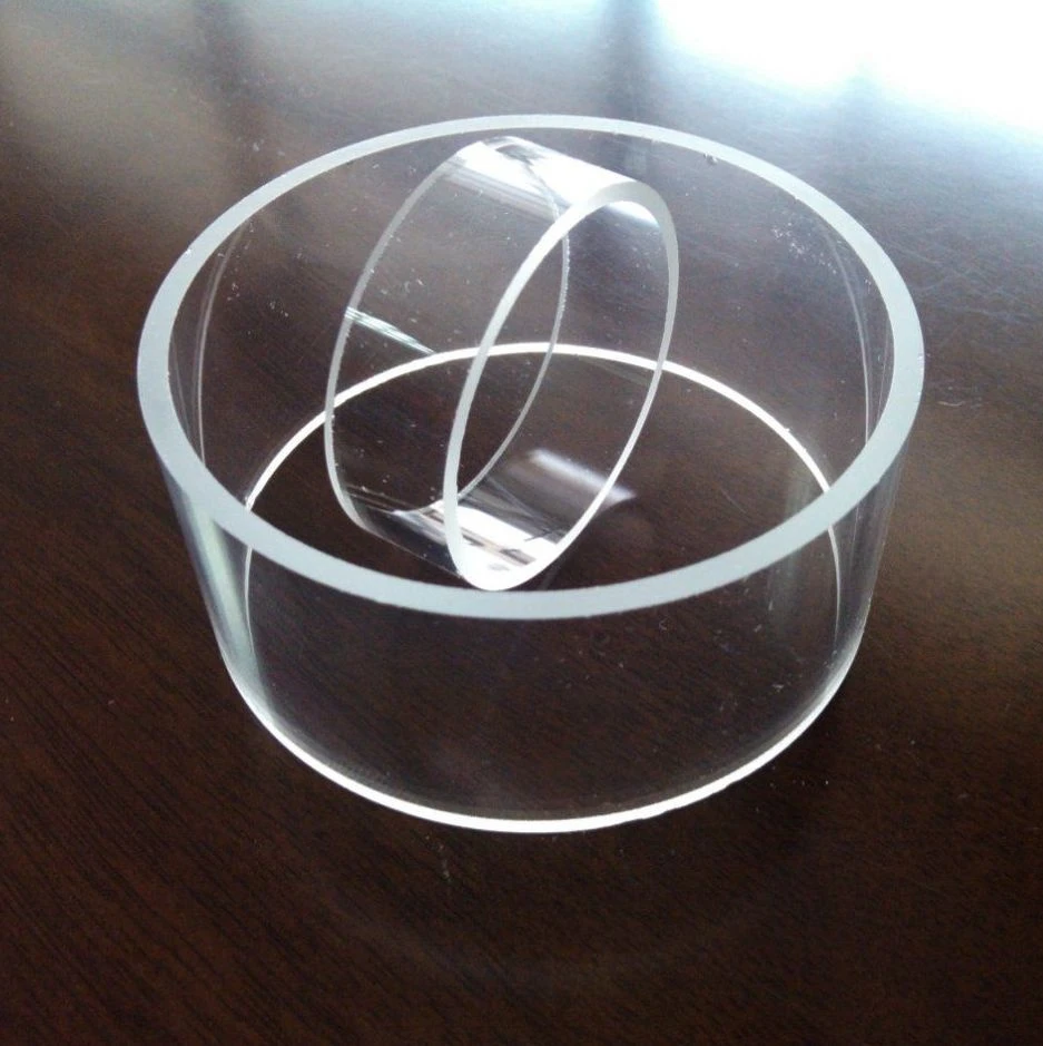
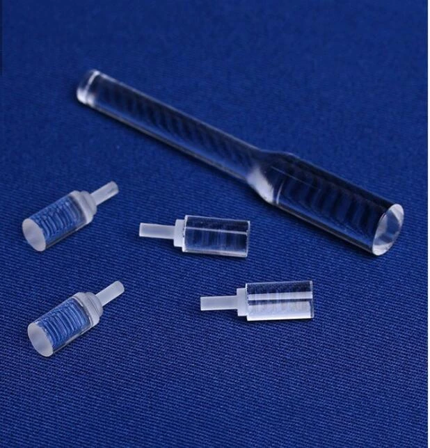
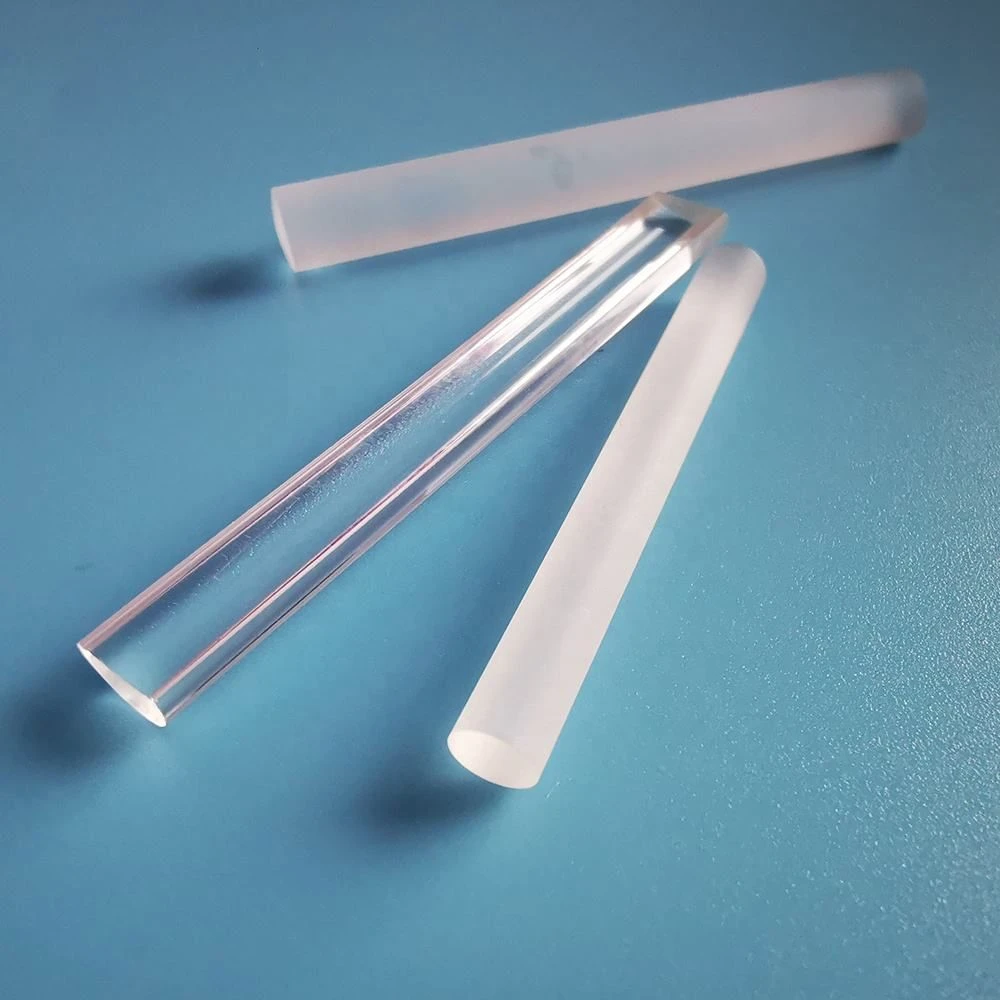
Model: WGP-3.
Overview
UV Visible Nir Swir Broadband Glass Quartz Substrate High Power Laser Polarizer is a waveplate / polariser / grating made from Eagle Xg. Optical / electrical data: wavelength 400-1600nm, transmittance Transmission values are measured at normal incidence at 450 nm, 550 nm, and 650 nm.. Surface quality 60/40 Scratch-Dig. Dimensions, material grade, coating and finish can be quoted to your drawing; the values above are the listed starting point.
Specifications
| Substrate | Eagle Xg |
|---|---|
| Surface Quality | 60/40 Scratch-Dig |
| Model NO. | WGP-3 |
| Dimensional Tolerance | ±0.2 mm |
| Polarization Wavelength Range | 400-1600nm |
| Extinction Ratio | 800:1(Average Over Wavelength Range) |
| Ar Coating | 450-1000nm |
| Angle of Incidence | 0° ± 20° |
| Thermal Expansion | 37.6 X 10⁻⁷/°C |
| Extinction ratio exceeding 800 | 1 ensures clean polarization separation |
| Transmission Reference | Transmission values are measured at normal incidence at 450 nm, 550 nm, and 650 nm. |
| Dimension Tolerance | Applies to length or diameter as applicable to the form factor. |
| CTE Scope | Coefficient of thermal expansion applies to the polarizer and glass cover only (excluding spacers/gaskets). |
| Reliability | Validated for 5,000 hours of continuous operation under specified conditions. |
| Deep silicon etching | aspect ratio 50:1 |
| ICP etching | dielectric-layer etching |
| RIE etching | dielectric-layer etching |
| Metal etching | dielectric-layer etching |
| Metals | Au, Ti, Ni, Cr, Al; |
| dielectric layers | TiN |
| Dielectric | TiO |
| Supplier | Kpl Controlled Environment Solution (Suzhou) Co., Ltd. |
Technical data
| Advantage | Description |
|---|---|
| Broad Wavelength Coverage | Polarization performance from 400 nm to 1600 nm, covering visible, near-IR, and SWIR bands |
| High Extinction Ratio | Extinction ratio exceeding 800:1 ensures clean polarization separation |
| High Transmission | Greater than 82% transmission maximizes optical throughput |
| Exceptional Thermal Stability | Operating temperature range from -40°C to 200°C for harsh environments |
| Wide Acceptance Angle | Performance maintained at incidence angles up to ±20° |
| Precision Surface Quality | Scratch/Dig specification of 60/40 ensures high optical clarity |
| Multiple Form Factors | Available in 12.5 mm square, 25 mm round, 25 mm square, and 50 mm square |
| Parameter | WP12.5L | WP25M | WP25L | WP50L |
| Substrate | EAGLE XG | EAGLE XG | EAGLE XG | EAGLE XG |
| Wavelength Range | 400–1600 nm | 400–1600 nm | 400–1600 nm | 400–1600 nm |
| Extinction Ratio | >800:1 | >800:1 | >800:1 | >800:1 |
| Transmission | >82% | >82% | ±2.5% | >82% |
| Form Factor | 12.5×12.5 mm | Ø25.0 mm | 25.0×25.0 mm | 50.0×50.0 mm |
| Dimension Tolerance | ±0.2 mm | +0.0/-0.1 mm | ±0.2 mm | ±0.2 mm |
| Clear Aperture | 10.5×10.5 mm | Ø19.0 mm | 21.0×21.0 mm | 48.0×48.0 mm |
| Thickness | 1.0 mm | 1.0 mm | 1.0 mm | 1.0 mm |
| Acceptance Angle | 0° ±20° | 0° ±20° | 0° ±20° | 0° ±20° |
| CTE | 37.6×10⁻⁷ /°C | 37.6×10⁻⁷ /°C | 37.6×10⁻⁷ /°C | 37.6×10⁻⁷ /°C |
| Surface Quality | 60/40 | 60/40 | 60/40 | 60/40 |
| Operating Temp. | -40 to 200°C | -40 to 200°C | -40 to 200°C | -40 to 200°C |
| Process | Substrate Size | Capability |
| MA8 photolithography | 4 / 6 / 8 inch | Minimum linewidth 1 μm |
| Stepper lithography | 4 inch | Minimum linewidth 0.7 μm |
| Electron-beam lithography (EBL) | 4 inch | Minimum CD 60 nm |
| Laser direct-writing & grayscale lithography | 4 / 6 / 8 inch | 3D grayscale exposure: 4095 levels; writing accuracy 250 nm |
| Dry etching | 4 / 6 / 8 inch | Deep silicon etching: aspect ratio 50:1 ICP etching: dielectric-layer etching RIE etching: dielectric-layer etching Metal etching: dielectric-layer etching |
| Wet etching | 4 / 6 / 8 inch | Silicon etching Metal etching |
| Magnetron sputtering | 4 / 6 / 8 inch | Metals: Au, Ti, Ni, Cr, Al; dielectric layers: TiN |
| Electron-beam evaporation | 4 / 6 / 8 inch | Metals: Au, Pt, Al, Cr, Ti, Ni, etc. |
| Atomic layer deposition (ALD) | 4 / 6 / 8 inch | Dielectric: TiO2, Al2O3, Ta2O5, HfO2, etc. |
| Nanoimprint lithography (NIL) | 4 / 6 / 8 inch | Minimum CD 50 nm |
| Anti-Sticking Treatment | 4 / 6 / 8 inch | CVD and spin-coating processes |
| Metrology & analytical measurement | Sample preparation | SEM, EDS, confocal microscopy, white-light interferometry, step profiler, IR microscopy, metallographic microscopy, etc. |
What to specify when you request a quote
- Material — listed as “Eagle Xg”; name the glass or crystal.
- Geometry — listed as “±0.2 mm”; give diameter, focal length or radii, angles and tolerances.
- Surface figure — listed as “60/40 Scratch-Dig”; quote surface figure (λ) and scratch-dig.
- Centring and edges — state centration and edge chamfer.
- Coating — listed as “450-1000nm”; list the band and reflectance or transmission target.
Engineering guides for this part
For material grades and coating options, see Fused Silica Windows for UV and Laser Optical Systems. How parts like this are machined and finished is covered in Laser Assisted Glass Cutting for Tight Tolerance Parts. For an application example, read How to Handle and Maintain Precision Glass Components in Laser Systems. A related standard product is Alkali-Free Glass Wafers.