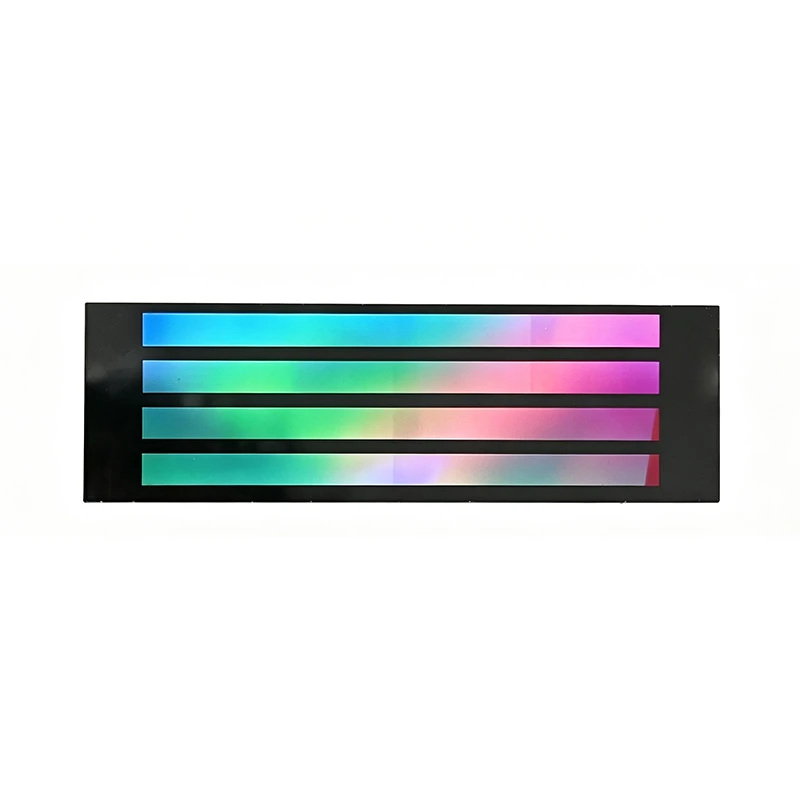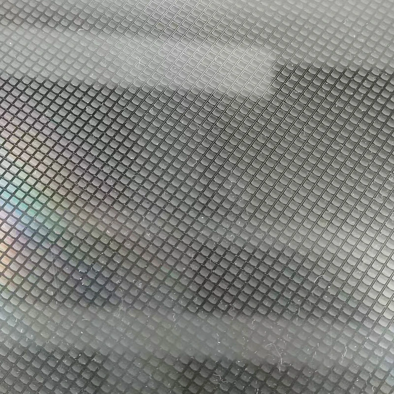
Model: Microfluidic subsrate-4.
Overview
Wafer Microfabrication Si/Glass Microfluidic Wafer with Etched Micro-Orifice for Drug Delivery & Lab-on-Chip is a microfluidic glass substrate made from Bf33 Glass Substrate+Silicon-Based. Dimensions, material grade, coating and finish can be quoted to your drawing; the values above are the listed starting point.
Specifications
| Material | Bf33 Glass Substrate+Silicon-Based |
|---|---|
| Model NO. | Microfluidic subsrate-4 |
| Format | 6-Inch Wafer |
| Maximum Aspect Ratio | 1:20 |
| Outlet Channel Width | 8 μm |
| Cylindrical Orifice Diameter | 10 μm |
| Orifice Diameter | > 5 μm |
| Important Disclaimer | We only supply pre-structured microfluidic wafer substrates. Finished atomization chips, modules or nebulizer devices are NOT |
| Deep silicon etching | aspect ratio 50:1 |
| ICP etching | dielectric-layer etching |
| RIE etching | dielectric-layer etching |
| Metal etching | dielectric-layer etching |
| Metals | Au, Ti, Ni, Cr, Al; |
| dielectric layers | TiN |
| Dielectric | TiO |
| Supplier | Kpl Controlled Environment Solution (Suzhou) Co., Ltd. |
Technical data
| Advantage | Description |
|---|---|
| High aspect ratio microstructure fabrication | UV nanoimprint lithography (UV-NIL) enables wafer-level batch fabrication of uniform microchannel / cylindrical orifice arrays with aspect ratio ≥5:1. Minimum outlet channel and orifice size >5 μm. |
| Composite substrate solution | 6-inch wafers combining BF33 glass substrate with silicon-based micro-nano structures, leveraging glass optical performance and silicon precision microfabrication capability. |
| Precisely controllable microfluidic profile | Fine tuning of microchannel sidewall geometry and vibration behavior, compatible with downstream SAW, ultrasonic and micro-heating aerosol generation systems. |
| Full-turnkey custom R&D service | Support microstructure simulation, process development, prototyping and volume manufacturing for 6-inch wafers. Custom microchannel layout, orifice dimension and substrate specifications available. |
| Wafer-level mass replication | UV-NIL replicates microstructures across the full 6-inch wafer with excellent batch uniformity for your mass production. |
| Flexible upstream substrate supply | Only pre-structured microfluidic wafer substrates are delivered. Customers carry out energy module integration and packaging independently to match their proprietary system design. |
| Process | Substrate Size | Capability |
| MA8 photolithography | 4 / 6 / 8 inch | Minimum linewidth 1 μm |
| Stepper lithography | 4 inch | Minimum linewidth 0.7 μm |
| Electron-beam lithography (EBL) | 4 inch | Minimum CD 60 nm |
| Laser direct-writing & grayscale lithography | 4 / 6 / 8 inch | 3D grayscale exposure: 4095 levels; writing accuracy 250 nm |
| Dry etching | 4 / 6 / 8 inch | Deep silicon etching: aspect ratio 50:1 ICP etching: dielectric-layer etching RIE etching: dielectric-layer etching Metal etching: dielectric-layer etching |
| Wet etching | 4 / 6 / 8 inch | Silicon etching Metal etching |
| Magnetron sputtering | 4 / 6 / 8 inch | Metals: Au, Ti, Ni, Cr, Al; dielectric layers: TiN |
| Electron-beam evaporation | 4 / 6 / 8 inch | Metals: Au, Pt, Al, Cr, Ti, Ni, etc. |
| Atomic layer deposition (ALD) | 4 / 6 / 8 inch | Dielectric: TiO2, Al2O3, Ta2O5, HfO2, etc. |
| Nanoimprint lithography (NIL) | 4 / 6 / 8 inch | Minimum CD 50 nm |
| Anti-Sticking Treatment | 4 / 6 / 8 inch | CVD and spin-coating processes |
| Metrology & analytical measurement | Sample preparation | SEM, EDS, confocal microscopy, white-light interferometry, step profiler, IR microscopy, metallographic microscopy, etc. |
What to specify when you request a quote
- Material — listed as “Bf33 Glass Substrate+Silicon-Based”; name the glass or quartz grade.
- Outline and thickness — listed as “10 μm”; give outline, thickness and tolerances.
- Holes, slots and features — dimension every hole and its position tolerance on the drawing.
- Edges — state edge finish and chamfer.
- Surface — state polish and flatness where they matter.
Engineering guides for this part
For material grades and coating options, see Borofloat Glass Wafers: Material & Coating Options for Substrates. How parts like this are machined and finished is covered in Glass Wafer Bonding for Microfluidic and MEMS Applications: Process Overview. For an application example, read Custom Precision Glass for Microfluidic and Biomedical Devices. Before sending a drawing, check Precision Glass Material Selection: Fused Silica vs Borosilicate & More. A related standard product is 4-inch Borofloat 33 Glass Wafers.