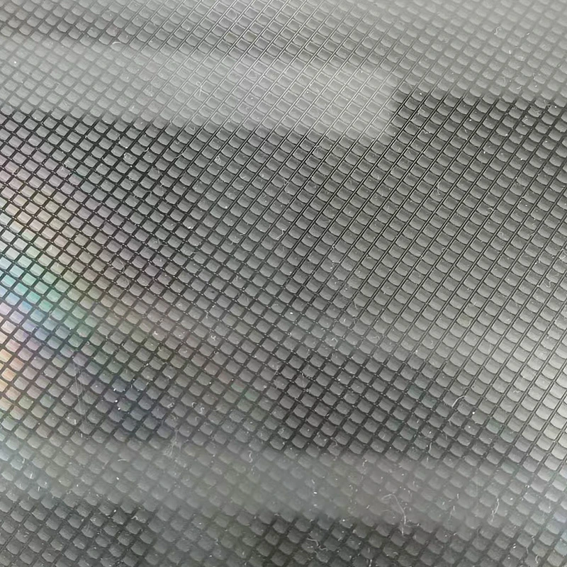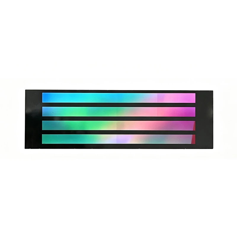
Model: NGS chip.
Overview
Patterned Nanowell Bare Core Substrate High-Throughput Ngs Sequencing Biochip Glass/Si Substrate OEM: a microfluidic glass substrate. Dimensions, material grade, coating and finish can be quoted to your drawing; the values above are the listed starting point.
Specifications
| Model NO. | NGS chip |
|---|---|
| Substrate Materials | Optical Glass/Monocrystalline Silicon/Silicon Carb |
| Base Substrate Types | Glass/Si/,Pdms |
| Critical Dimensions (CD) | ≥ 50 Nm |
| Minimum Pore Size | 100 Nm |
| Minimum Period | 200 Nm |
| OEM/ODM custom manufacturing | array density, probe layout, and substrate material are tailored to each customer's platform requirements. |
| Deep silicon etching | aspect ratio 50:1 |
| ICP etching | dielectric-layer etching |
| RIE etching | dielectric-layer etching |
| Metal etching | dielectric-layer etching |
| Metals | Au, Ti, Ni, Cr, Al; |
| dielectric layers | TiN |
| Dielectric | TiO |
| Supplier | Kpl Controlled Environment Solution (Suzhou) Co., Ltd. |
Technical data
| Process | Substrate Size | Capability |
| MA8 photolithography | 4 / 6 / 8 inch | Minimum linewidth 1 μm |
| Stepper lithography | 4 inch | Minimum linewidth 0.7 μm |
| Electron-beam lithography (EBL) | 4 inch | Minimum CD 60 nm |
| Laser direct-writing & grayscale lithography | 4 / 6 / 8 inch | 3D grayscale exposure: 4095 levels; writing accuracy 250 nm |
| Dry etching | 4 / 6 / 8 inch | Deep silicon etching: aspect ratio 50:1 ICP etching: dielectric-layer etching RIE etching: dielectric-layer etching Metal etching: dielectric-layer etching |
| Wet etching | 4 / 6 / 8 inch | Silicon etching Metal etching |
| Magnetron sputtering | 4 / 6 / 8 inch | Metals: Au, Ti, Ni, Cr, Al; dielectric layers: TiN |
| Electron-beam evaporation | 4 / 6 / 8 inch | Metals: Au, Pt, Al, Cr, Ti, Ni, etc. |
| Atomic layer deposition (ALD) | 4 / 6 / 8 inch | Dielectric: TiO2, Al2O3, Ta2O5, HfO2, etc. |
| Nanoimprint lithography (NIL) | 4 / 6 / 8 inch | Minimum CD 50 nm |
| Anti-Sticking Treatment | 4 / 6 / 8 inch | CVD and spin-coating processes |
| Metrology & analytical measurement | Sample preparation | SEM, EDS, confocal microscopy, white-light interferometry, step profiler, IR microscopy, metallographic microscopy, etc. |
What to specify when you request a quote
- Material — listed as “Optical Glass/Monocrystalline Silicon/Silicon Carb”; name the glass or quartz grade.
- Outline and thickness — listed as “≥ 50 Nm”; give outline, thickness and tolerances.
- Holes, slots and features — dimension every hole and its position tolerance on the drawing.
- Edges — state edge finish and chamfer.
- Surface — state polish and flatness where they matter.
Engineering guides for this part
For material grades and coating options, see BF33 Glass for Microfluidic Chips: Properties, Coatings & Selection Guide. How parts like this are machined and finished is covered in Glass Wafer Bonding for Microfluidic and MEMS Applications: Process Overview. For an application example, read Custom Precision Glass for Microfluidic and Biomedical Devices. A related standard product is Custom Glass Microfluidic Chip.
FAQ
What should I include in a quote request? expand_more
Include material, outline and thickness, holes, slots and features, edges and surface, plus quantity and a drawing if the part is custom.