
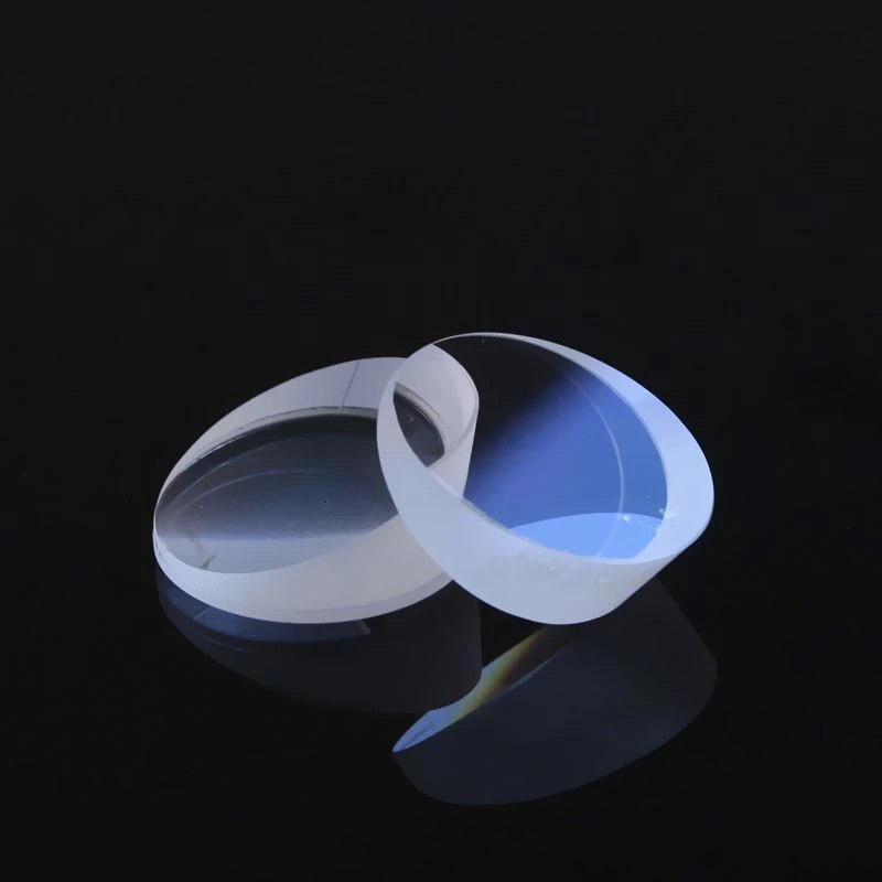
Product type: Thin Film Filter. Application: Lighting, Medical, Optical, Photography. Model: AW517.
Overview
Wholesale Quality 4inch 2inch Sapphire Wafer 10X10mm 5X5mm Sapphire Substrate Wafer is a sapphire / specialty wafer made from Glass. Listed geometry: diameter 0/-0.1, size Customized, thickness 0.5mm-1mm. Optical / electrical data: wavelength 632.8nm. Coating: Customized. Listed for Lighting, Medical, Optical and Photography applications. Dimensions, material grade, coating and finish can be quoted to your drawing; the values above are the listed starting point.
Specifications
| Material | Glass |
|---|---|
| Type | Thin Film Filter |
| Shape | Customized |
| Coating | Customized |
| Clear Aperture | >90% |
| Usage | Lighting, Medical, Optical, Photography |
| Model NO. | AW517 |
| Thickness Range | 0.5mm-1mm |
| Color | Customize |
| Angle of incidence | Customize |
| Focal Length Tolerance | < ± 1% |
| Thickness Tolerance | Thickness Tolerance ± 0.1 |
| Eccentricity | 3′ |
| Designed Wavelength | 632.8nm |
| Scratch/Dig | 60/40 |
| Diameter Tolerance | 0/-0.1 |
| Coating Coating | Ar or Bbar |
| Dimensions | Customized |
| Colors | Customized |
| a=4.758 Å,Å c=12.991 Å, c | a=2.730 |
| Filter glass prepared | – With processessed edges |
| Standard formats with non-processed edges | Plate sizes 165 x 165 + 3-0 mm |
| Aspheric Lenses | Advantages & Disadvantages In a nutshell, aspheric lenses have the following advantages: |
| Applications | 1 . Correcting Astigmatism |
| Supplier | Fujian Allwin Technology Co., Ltd. |
Technical data
| GENERAL | |||
| Chemical Formula | Al2O3 | ||
| Crystal Stucture | Hexagonal System ((hk o 1) | ||
| Unit Cell Dimension | a=4.758 Å,Å c=12.991 Å, c:a=2.730 | ||
| PHYSICAL | |||
| Metric | English (Imperial) | ||
| Density | 3.98 g/cc | 0.144 lb/in3 | |
| Hardness | 1525 – 2000 Knoop, 9 mhos | 3700° F | |
| Melting Point | 2310 K (2040° C) | ||
| STRUCTURAL | |||
| Tensile Strength | 275 MPa to 400 MPa | 40,000 to 58,000 psi | |
| at 20° | 400 MPa | 58,000 psi (design min.) | |
| at 500° C | 275 MPa | 40,000 psi (design min.) | |
| at 1000° C | 355 MPa | 52,000 psi (design min.) | |
| Flexural Stength | 480 MPa to 895 MPa | 70,000 to 130,000 psi | |
| Compression Strength | 2.0 GPa (ultimate) | 300,000 psi (ultimate) |
| Size | Φ1.0~7mm | Φ8.0~20mm | Φ20.0~40mm | Φ40.0~60mm |
| PV | 0.2um | 0.3um | 0.5um | <1um |
| Eccentricity | <=3um | <=5um | <=5um | <=8um |
| Center Thickness Tolerance | ±0.015mm | ±0.020mm | ±0.025mm | ±0.050mm |
| Diameter Tolerance | ±0.015mm | ±0.015mm | ±0.015mm | ±0.030mm |
| Surface Quality | 40/20 | |||
| Surface Roughness | >20nm | |||
| RMS | According to the optical system | |||
| Material | CDGM, NHG, customer Requirements |
What to specify when you request a quote
- Diameter and flat / notch — listed as “0/-0.1”; state diameter, flat or notch and their tolerances.
- Thickness and TTV — listed as “0.5mm-1mm”; give thickness, its tolerance and total thickness variation.
- Polish and roughness — specify single- or double-side polish and roughness.
- Flatness, bow and warp — quote flatness, bow and warp limits.
- Material grade — listed as “Glass”; name the grade (JGS1/JGS2, Borofloat 33, alkali-free, sapphire orientation).
Engineering guides for this part
For material grades and coating options, see Fused Quartz Wafer Substrate Selection: Materials & Coatings for Semiconductor and Optical Systems. How parts like this are machined and finished is covered in Precision Glass Hole Machining for MEMS and Wafer Parts.


