
Key Takeaways
- Fused silica wafers excel in appliance electronics due to their high optical clarity, thermal stability, and chemical resistance.
- Material grades like JGS1 and JGS2 address specific UV transmission needs while balancing cost.
- Surface quality (scratch-dig 20-10) and precise dimensional tolerances (TTV <5 µm) are critical for coating adhesion and assembly.
- Anti-reflective and conductive coatings expand functional capabilities for touchscreens and sensor windows.
- Working with an ISO-certified supplier ensures reliable material traceability and cleanroom packaging.
The Application Goal and Constraints: Reliable Optics in Harsh Appliance Environments
How can you maintain consistent touchscreen responsiveness, sensor accuracy, and display clarity in a smart oven that cycles from room temperature to 500 °F, or in a washing machine exposed to humidity and detergents? Precision appliance electronics demand materials that survive thermal shock, resist chemical attack, and preserve optical integrity over years of daily use. Whether it’s a through-glass interface, an infrared sensor window, or a protective cover for a diagnostic display, the glass component must combine flatness for lamination, transmission for sensor signals, and dielectric strength for electrical isolation—often within tight mechanical envelopes.
How Fused Silica Wafers Meet These Requirements
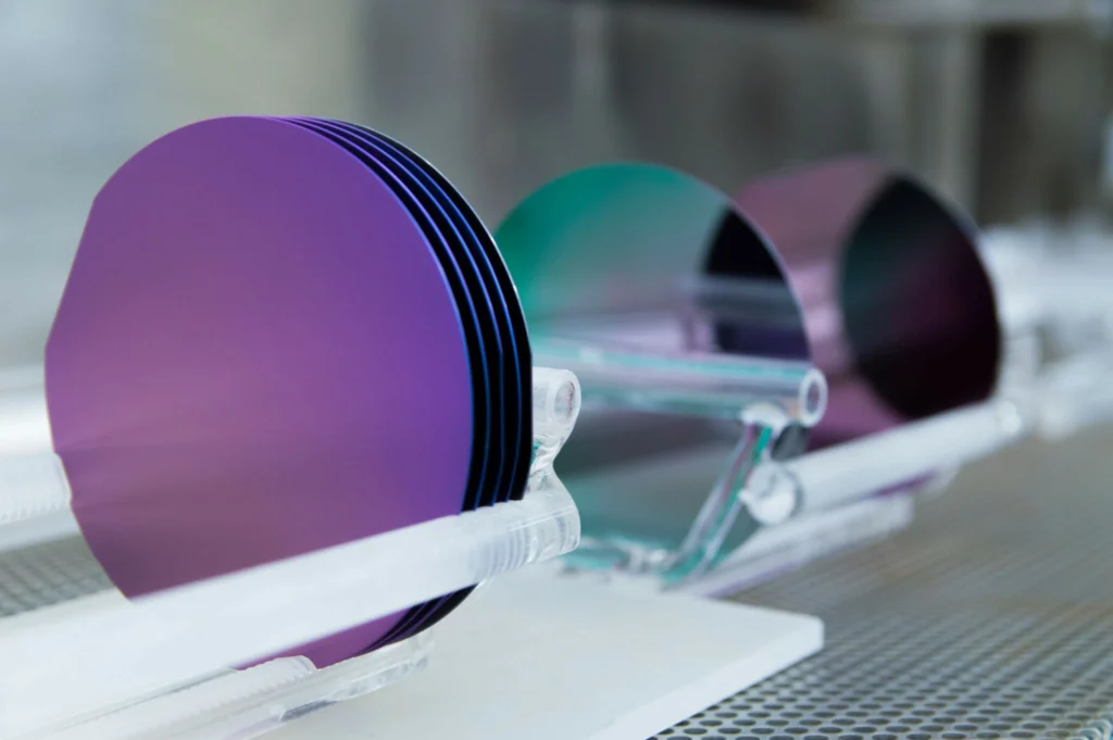
A fused silica wafer is a high-purity, amorphous silicon dioxide substrate created by melting and resolidifying silica in a controlled process. The result is a glass with near-zero thermal expansion (CTE around 0.55 × 10⁻⁶/K), excellent thermal shock resistance, and broadband transparency from deep UV through the near-infrared. Unlike soda-lime or borosilicate alternatives, fused silica maintains its shape and optical properties through rapid temperature swings—critical for cooking appliances, steam-cleaned interfaces, and outdoor electronics. Its high chemical inertness withstands cleaning agents and process chemicals, while its inherent electrical insulation prevents short circuits in proximity to live components. These attributes make fused silica wafers a reliable foundation for appliance electronics glass, serving as touch panel substrates, protective windows, and optical sensor covers.
Selection Criteria for Appliance Electronics
When specifying a precision glass wafer for an appliance application, engineers typically evaluate:
- Optical transmission: Visible-range clarity often exceeds 90%, but IR- or UV-blocking coatings may be needed to protect internal electronics or manage sensor wavelengths.
- Thermal expansion match: Fused silica’s low CTE reduces stress when bonded to ceramic or silicon parts, but may require compliant adhesives when framing with higher-expansion metals.
- Surface quality and flatness: A polished surface (typically λ/4 or better) supports uniform lamination of touch films and anti-fingerprint coatings, and minimizes distortion for camera or LIDAR windows.
- Chemical durability: Resistance to household acids, alkalis, and solvents ensures long-term optical quality even with frequent cleaning.
- Compliance: Confirm RoHS, REACH, and any appliance-specific safety standards for the intended market.
A Realistic Project Scenario: Smart Oven Interface
A manufacturer developing a high-end built-in oven wants a full-color TFT display behind a seamless glass panel, plus an inline camera for food monitoring. The glass must withstand direct heat from the oven cavity, cooling from ventilation fans, and occasional spills. After evaluating tempered soda-lime (which warps under prolonged heat) and borosilicate (sufficient for thermal but with lower optical homogeneity), the team selects a UV-grade fused silica wafer, 200 mm diameter × 0.7 mm thick. The wafer is diamond-cut to final shape, edge-ground for safe handling, and double-side polished to Ra < 1 nm for direct bonding of the display and touch layers. An AR coating on both sides boosts transmission to >95%, while an oleophobic top coat resists fingerprints. The manufacturer integrates the assembly using a flexible adhesive that accommodates the CTE difference with the stainless steel frame. The result is a crisp, responsive interface that remains reliable across the appliance’s service life.
Planning for Sizing, Tolerance Stack-Up, Coating, and Integration
Fused silica wafers are available in standard diameters from 2 inch to 300 mm and custom shapes. Thicknesses often range from 0.3 mm for lightweight overlays to 1.5 mm for robust windows. In an appliance assembly, account for the cumulative tolerances of the glass, the adhesive bondline, and the housing features. Specify flatness and thickness variation to match the bonding process: an interferometrically verified surface ensures uniform lamination. Typical coatings include anti-reflective (single- or multi-layer), conductive ITO for touch functionality, and easy-clean layers. Work with your glass processor to define edge profiles (bullnose, chamfer) and dimensional callouts. For logistics, wafers are usually shipped in cleanroom-grade packaging with interleaved films to prevent scratching. Discuss packaging formats for automated pick-and-place if high-volume assembly is planned.
Discuss Your Project Requirements
Every appliance integration presents a unique set of mechanical, optical, and environmental demands. Our applications team can help you translate your performance targets into a tailored glass wafer specification—from material grade and coating design to shape and tolerance definition. Contact us with your project details, and we will propose a precision glass solution that aligns with your production timeline and budget.
Fused Silica Wafer Attributes for Appliance Electronics
Fused silica wafers deliver exceptional optical transmission from deep UV through near-IR, combined with near-zero thermal expansion and high chemical durability—properties that directly support high-precision appliance displays, sensor windows, and touch interfaces. In appliance electronics, these fused silica wafers serve as protective cover lenses, capacitive touch substrates, and optical filter carriers where consistent performance under varying humidity and temperature is non-negotiable.
Optical Performance and Transmission
Key to appliance displays is broadband visible transparency (>90% typical) along with controlled UV blocking or transmission depending on the appliance function. Fused silica’s low auto-fluorescence and minimal birefringence ensure crisp image quality and reliable sensor readings. Standard thicknesses for appliance-grade wafers range from 0.3 mm to 2.0 mm, supporting both rigid and slightly flexible assemblies.
Thermal and Mechanical Stability
With a coefficient of thermal expansion (CTE) near 0.55 × 10⁻⁶/K, fused silica wafers maintain flatness across wide temperature swings—critical for oven or refrigeration appliance interfaces. Their hardness resists scratching from daily cleaning, while precise edge chamfering reduces chipping during automated assembly.
Chemical Robustness
Resistance to common household cleaners, oils, and moisture prevents surface degradation over the appliance’s service life. This durability reduces warranty claims linked to optical clouding or coating delamination.
Material Grades and Substrate Options
Selecting the appropriate fused silica grade balances UV requirements with cost. JGS1 (UV-grade) offers high transmission down to 185 nm, ideal for appliances using UV sterilization or spectroscopy-based sensors. JGS2 (optical grade) provides excellent visible transmission at a lower cost for standard display covers. For moderate UV transparency, full-spectrum fused silica wafers bridge the two. Suppliers often stock 100 mm, 150 mm, and 200 mm diameter wafers, with custom shapes—square, rectangular, or with notches—available through CNC machining. For diced wafer segments, advanced glass wafer dicing techniques ensure clean edges and minimal chipping. Thickness tolerances as tight as ±10 µm and total thickness variation (TTV) under 5 µm support multi-layer bonding and optical path alignment.
Surface Quality and Coating Capabilities
Surface finish is specified by scratch-dig (e.g., 20-10 per MIL-PRF-13830) and flatness (λ/4 or better at 633 nm). Double-sided polishing routinely achieves Ra < 1 nm, which is essential for optical bonding and thin-film coating uniformity. Anti-reflective (AR) coatings can push transmission above 99% in the visible spectrum, while transparent conductive coatings like ITO add touch functionality without sacrificing clarity. Oleophobic easy-clean layers further enhance user experience in appliance interfaces.
Key Specifications at a Glance
- JGS1 UV-grade fused silica transmits above 90% at 185 nm.
- Fused silica CTE of 0.55 × 10⁻⁶/K ensures negligible thermal distortion.
- Surface flatness up to λ/10 is achievable through double-sided polishing.
- Anti-reflective coatings can boost transmission to over 99% in the visible range.
- Standard sizes include 100 mm, 150 mm, and 200 mm wafers, with custom geometries available.
Supply Chain and Integration Support
For high-volume appliance programs, the precision glass supplier’s quality management system is as critical as material purity. Look for partners with ISO 9001 certification who can provide full material traceability and certificates of conformance per batch. In-process inspections using non-contact optical profilers and laser interferometers verify flatness, surface roughness, and dimensional accuracy before shipment. Packaging in cleanroom-compatible cassettes with interleaved films protects wafers until assembly, and custom packaging options—such as Gel-Pak trays or tape-and-reel for automated pick-and-place—streamline your production line.
To begin specifying a fused silica wafer for your next appliance design, contact our engineering team. Share your optical, dimensional, and environmental requirements, and we’ll propose a substrate configuration with recommended coating and edge treatment. A quick technical review can prevent integration delays and ensure your appliance meets performance and reliability targets.
| Aspect | Key Details | Why It Matters |
|---|---|---|
| Material Choices | Fused silica (JGS1, JGS2), borosilicate, sapphire | Matches optical, thermal, and cost targets per application |
| Optical Transmission | UV to IR; >90% visible typical | Ensures display clarity and sensor accuracy |
| Thermal Stability | CTE ~0.55 × 10⁻⁶/K | Maintains flatness in varying appliance environments |
| Surface Quality | Scratch-dig 20-10 to 40-20; λ/10 flatness | Affects optical performance and coating adhesion |
| Coatings | AR, ITO, easy-clean, UV-block | Enhance function: anti-reflection, conductivity, cleanability |
| Typical Tolerances | Thickness ±10 µm, TTV <5 µm, size ±0.1 mm | Supports high-volume automated assembly |
| Compliance | RoHS, REACH; ISO 9001 facilities | Meets regulatory and quality management expectations |
Frequently Asked Questions
What makes fused silica wafers better than soda-lime glass for appliance touch panels?
Fused silica offers superior thermal stability with a near-zero coefficient of thermal expansion, preventing warping under temperature changes. It also provides higher visible transparency and greater resistance to scratches and chemical cleaners, making it ideal for premium appliance interfaces.
Which fused silica grade should I choose for a UV sterilization appliance window?
JGS1 grade fused silica is recommended for UV sterilization applications because it offers high transmission down to 185 nm. For appliances that require deep-UV transparency without significant cost increase, JGS1 is the preferred choice, while JGS2 suffices for visible-only applications.
How do anti-reflective coatings on fused silica wafers improve appliance display readability?
Multi-layer AR coatings reduce surface reflectance from about 4% per side to less than 0.5%, significantly boosting transmitted light and minimizing glare. This enhances screen readability under bright kitchen or laundry room conditions.
What typical thickness tolerances are achievable for fused silica wafers in high-volume appliance production?
Precision lapping and polishing can achieve thickness tolerances of ±10 µm and total thickness variation (TTV) under 5 µm. These tight tolerances ensure consistent optical path lengths and reliable bonding in automated assembly lines.
Can fused silica wafers be custom shaped for non-rectangular appliance displays?
Yes, fused silica wafers can be CNC-machined or laser-cut into circular, elliptical, or freeform shapes with edge chamfers to prevent chipping. Custom shapes are fully supported for both prototyping and volume production.