
Key Takeaways
- Fused silica wafers require careful dicing parameter control to avoid micro-cracks and chipping, while borofloat offers a more forgiving fracture behavior.
- Scribing and breaking, blade dicing, and laser-based methods each suit different wafer thicknesses and production volumes.
- In-line quality checks monitor edge quality, die strength, and dimensional accuracy to ensure consistent output for bulk orders.
- A controlled cleanroom environment and proper dicing tape/film selection significantly impact yield.
Precision Glass Wafer Dicing: A Complete Process Overview
The single most critical factor in glass wafer dicing is matching the method to the material. Fused silica and borofloat respond very differently to mechanical and thermal stress, so the process must be tightly controlled to deliver clean, chip-free die with high edge strength.
Key Process Facts
- Fused silica (JGS1, JGS2) requires low-force scribing and controlled break techniques to limit micro-cracks.
- Borofloat 33 offers more forgiving fracture behavior, allowing higher throughput mechanical dicing.
- Laser-based dicing (ablation, stealth) reduces edge chipping for both materials but demands careful parameter tuning.
- Post-dicing edge grinding and cleaning steps are essential for achieving final die quality.
Base Glass Substrates for Dicing: Fused Silica and Borofloat
Dicing success starts with substrate selection. The two primary materials covered here are fused silica and borofloat glass. Fused Silica Glass Wafers (2–12″, JGS1/JGS2) are typically specified in optical and semiconductor applications for their high UV transmission and thermal stability. Fused silica grades like JGS1 (UV-grade) and JGS2 (standard-grade) both exhibit a brittle fracture behavior that requires careful dicing parameter control to avoid cracking and chipping. borofloat 33 glass wafers 5 are a borosilicate float glass with excellent flatness and a lower hardness than fused silica. This makes them more amenable to higher-speed mechanical dicing, though edge quality can still be compromised if feed rates are too aggressive. For detailed guidance on selecting the right fused silica grade, see our resource on Choosing Between JGS1 and JGS2 Fused Silica.
Step-by-Step Dicing Production Stages
Pre-Dicing Wafer Preparation: Grinding, Lapping, and Polishing
Before dicing, wafers often undergo thinning and planarization. Backside grinding reduces substrate thickness to a target TTV (total thickness variation), followed by lapping to remove sub-surface damage. Polishing delivers the final surface finish, typically Ra < 1 nm for fused silica, which is critical for subsequent bonding or coating processes. A polished surface also reduces stress concentration points during dicing.
Scribing and Cutting: Mechanical and Laser Methods
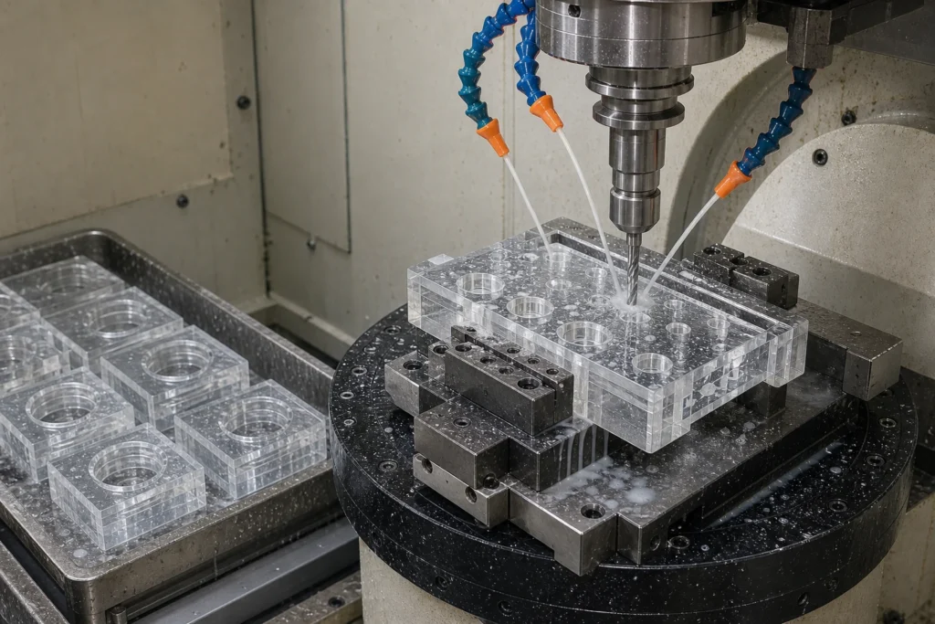
The core dicing step can be executed through several techniques. Mechanical scribing uses a diamond tip to create a shallow crack along the desired cut line; this is the most common method for borofloat wafers up to 500 µm thick. For fused silica and thicker wafers, saw-based dicing with a high-speed diamond blade provides deeper cuts and is often preferred for 300mm glass wafer dicing where high volume is required. Laser scribing (e.g., CO2 or UV laser) offers a non-contact alternative that reduces edge chipping, especially for delicate fused silica. Stealth dicing, which creates a modified layer inside the wafer with a focused laser, enables separation without surface debris and minimal kerf loss.
Breaking and Die Separation
Once scribe lines are created, the wafer is separated into individual die using a controlled breaking process. Roller break systems apply precise pressure to propagate the crack along the scribe line, while three-point breaking may be used for thicker wafers. The break step must be calibrated to the material’s brittleness: fused silica typically requires a lower break force and slower crack propagation to avoid angular chipping.
Post-Dicing Processes: Edging, Drilling, and Coating
After separation, die edges often require edge grinding to remove sharp corners and micro-fractures. CNC drilling or routing may be employed if vias or custom shapes are needed. Protective coatings such as metal or dielectric films are sometimes deposited before or after dicing to enhance die strength or provide optical functionality.
Strengthening and Tempering (If Required)
For applications demanding high flexural strength, a chemical tempering step can be applied, though this is less common for diced glass die. Thermal tempering is generally unsuitable due to the small form factor.
Final Cleaning and Inspection
A multi-stage cleaning process using ultrasonic, megasonic, and spin-rinse drying removes dicing debris, tape residues, and particles. This is essential before shipment, as even microscopic contamination can impair downstream die attach or optical performance.
Dicing Equipment and Quality-Enhancing Techniques
High-quality dicing relies on rigid, vibration-damped equipment. CNC dicing saws with automatic blade wear compensation maintain cut consistency across thousands of dice. Dual-spindle machines allow simultaneous rough and finish cutting. For laser processes, magnetron sputtering may be used to deposit a protective layer before scribing. All precision glass dicing operations should be performed in a cleanroom (ISO Class 7 or better) to prevent particulate contamination.
In-Line Quality Checkpoints During Dicing
Critical specifications are verified at multiple points. Dimensional checks measure die size and kerf width to within ±5–10 µm using automated optical inspection. Flatness and TTV are confirmed via interferometry. Surface quality is inspected under high-intensity lighting for scratches and digs per MIL-PRF-13830 or similar standards. Statistical process control tracks edge chipping rates, die strength via ring-on-ring tests, and optical transmission for coated lots.
Scalability and Consistency for High-Volume Orders
For bulk orders, process consistency is paramount. Multiple dicing saws can be run in parallel with identical recipes, and automated wafer loading/unloading reduces cycle time. Real-time monitoring of spindle current and blade wear helps maintain tight control. Typical order volumes can range from prototype lots of 10–25 wafers to full production runs of 500+ wafers per week, with lead times scaling accordingly.
Request a Detailed Factory Process Overview
Every precision glass dicing project requires a custom approach. To discuss your specific fused silica or borofloat wafer requirements—including thickness, die size, and quality targets—contact our engineering team for a detailed process overview and quotation.
| Process Stage | Purpose | Key Techniques/Methods | Quality Metrics |
|---|---|---|---|
| Wafer Preparation | Achieve target thickness and flatness before dicing | Grinding, lapping, polishing | TTV < 3 µm, Ra < 1 nm |
| Scribing | Create precise separation lines | Diamond scribe, laser scribe, stealth dicing | Scribe depth uniformity, minimal chipping |
| Breaking/Die Separation | Separate die cleanly | Roller break, three-point break | Edge quality, die strength > 50 MPa |
| Post-Processing | Refine edges and add features | Edge grinding, CNC drilling, coating | Dimensional tolerance ±10 µm, coating integrity |
| Cleaning & Inspection | Eliminate contamination | Ultrasonic, megasonic, spin-rinse drying | ≤ 0.3 particles/cm² > 0.5 µm |
Frequently Asked Questions
What are the main challenges when dicing fused silica wafers compared to borofloat?
Fused silica is harder and more brittle, making it prone to micro-cracks and edge chipping if feed rates or scribe forces are too high. Borofloat has a lower hardness and more ductile fracture, allowing faster mechanical dicing but still requiring careful calibration to avoid breakage.
Which dicing method is best for 300mm glass wafers?
For 300mm glass wafers, saw-based dicing with a diamond blade is common for high-volume production, though laser scribing or stealth dicing can offer superior edge quality and reduced chipping, especially for thin or fragile substrates.
How does glass wafer dicing differ from silicon wafer dicing?
Glass is amorphous and more brittle than crystalline silicon, so it does not cleave along crystal planes. Dicing must rely on scribing and breaking or pure mechanical/laser cutting, with greater sensitivity to feed rate and blade specification to avoid cracks.
What tolerances can be expected in glass wafer dicing?
Typical dimensional tolerances for diced glass die are in the range of ±5 to ±10 µm, with edge chipping controlled to below 50 µm. Tighter tolerances require optimized equipment and process control.
How is edge chipping minimized during fused silica wafer dicing?
Edge chipping is minimized by using a high-quality diamond blade with appropriate grit size, controlling feed rate and spindle speed, applying a protective coating before dicing, and using a two-step cut process with a rough cut followed by a finish cut.