
Stacked Fused Silica Wafers Form Ion Trap with Over 100 Ions
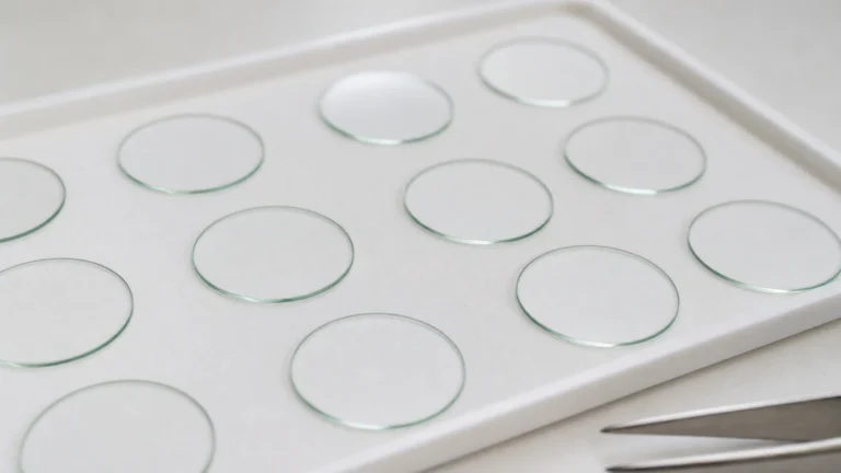
A precision ion trap built from stacked fused silica wafers has successfully confined more than 100 ions in a two-dimensional pattern, opening new avenues for flexible quantum simulation architectures. The design, reported by researchers on social media, achieves high radial frequencies and relies on straightforward fabrication methods that could simplify the mass production of trapped-ion quantum hardware.
Traditional ion traps often employ complex electrode geometries fabricated on insulating substrates using multi-step lithographic processes. By contrast, the new approach uses fused silica machining to create precise three-dimensional structures in stacked wafers. This method streamlines assembly while maintaining the electrical and thermal stability required for ion confinement. The result is a scalable platform that supports large ion arrays, a critical milestone for quantum simulation of many-body systems.
Trapped ions are among the most promising qubit technologies due to their long coherence times and high-fidelity gate operations. Arranging them in two-dimensional grids enhances connectivity and enables the study of complex lattice models. With over 100 ions, the system enters a regime where classical simulation becomes intractable, offering a genuine quantum advantage in simulating materials, chemical reactions, and fundamental physics. While superconducting qubits have garnered attention for achieving high qubit counts, trapped ions offer superior coherence times and gate fidelities, making them especially attractive for simulation tasks that require deep circuits.
Market Implications for Quantum Hardware
The quantum computing industry is experiencing rapid growth, with trapped-ion systems competing alongside superconducting and photonic platforms. Companies like IonQ and Quantinuum have already commercialized ion-trap processors, and the demand for more qubits with lower error rates continues to rise. A fabrication process based on fused silica wafers could significantly reduce manufacturing costs and accelerate production cycles. The global fused silica wafer market, valued at hundreds of millions of dollars, already serves the semiconductor and optics industries, providing a ready supply chain for quantum hardware manufacturers.

By leveraging standard wafer sizes and fused silica dicing techniques, the ion trap design aligns with existing microelectronics infrastructure. This compatibility opens the door to wafer-scale integration, where multiple trap arrays are fabricated on a single substrate and diced into individual chips. Such economies of scale could bring down the per-qubit cost, making quantum simulation more accessible to research laboratories and eventually to enterprise customers. The fused silica approach could also enable three-dimensional trap geometries through wafer stacking, potentially supporting even larger arrays.
Technical and Standards Implications
Fused silica offers a unique combination of properties that make it ideal for ion traps: a low coefficient of thermal expansion, high electrical resistivity, and excellent dielectric strength. These traits ensure that the traps maintain dimensional stability under varying temperature conditions and can withstand the high electric fields needed for ion confinement. Furthermore, fused silica is transparent across a broad optical spectrum, facilitating the integration of laser cooling and state readout optics directly through the trap substrate.
From a standards perspective, the use of established wafer formats (e.g., 100 mm or 150 mm diameter, standard thicknesses) could catalyze the development of industry-wide specifications for quantum ion traps. Precision machining methods such as laser ablation and CNC milling, already well-characterized for fused silica, enable repeatable production of electrode features with micron-level accuracy. Standard wafer dicing processes, such as those used in the semiconductor industry, can be adapted to singulate individual traps with minimal edge chipping, preserving the precision of the machined electrodes. This paves the way for standardized trap designs that could be shared across research groups and commercial entities, much as semiconductor process design kits (PDKs) have done for integrated circuits.
What to Watch Next
While the initial demonstration proves the viability of the stacked-wafer ion trap, several performance metrics remain to be evaluated. Key among these are the fidelity of single- and two-qubit gates, the impact of electrode surface roughness on ion heating rates, and the long-term stability of trapped arrays. Researchers will likely publish a detailed characterization, including coherence times and error benchmarks, in a peer-reviewed journal.
Another area to monitor is the integration of optical components directly into the fused silica stack. Because the material is transparent, it is possible to etch waveguides or microlenses into the same substrate, potentially enabling a fully integrated optical interface for individual ion addressing. Such advances would further reduce system complexity and align with the trend toward photonic integration in quantum computing.
| Aspect | Details |
|---|---|
| Material | Precision-machined fused silica wafers |
| Fabrication technique | Stacked wafer assembly using CNC/laser machining |
| Ion capacity | Over 100 ions in 2D arrays |
| Target application | Quantum simulation of many-body systems |
| Key advantage | Simple fabrication, high radial frequencies |
| Industry compatibility | Standard semiconductor wafer supply chain |
A detailed performance analysis, including gate fidelities and error rates, is expected in an upcoming journal submission. Further announcements from the research group may also appear at quantum computing conferences later this year.
Why This Matters
This breakthrough merges the maturity of fused silica microfabrication with trapped-ion quantum computing, potentially lowering the barrier to large-scale quantum simulators. By harnessing standard wafer-scale processes, the design points toward cost-effective, manufacturable quantum hardware, opening doors to simulating complex materials and chemical systems that are beyond classical computers.
FAQ
What is the innovation behind this ion trap?
Researchers used precision-machined fused silica wafers stacked together to create an ion trap, simplifying the fabrication process compared to traditional methods. This design supports over 100 ions arranged in a two-dimensional array, enabling flexible configurations for quantum simulation experiments.
Why is a 2D array of over 100 ions significant for quantum simulation?
Larger ion arrays allow for more complex simulations of quantum systems, such as lattice models in materials science or molecular interactions. With 100+ ions, the system can perform calculations that are difficult or impossible for classical computers, providing a valuable tool for scientific discovery.
What role does fused silica play in the trap’s performance?
Fused silica offers high thermal stability, excellent electrical insulation, and optical transparency, which are essential for maintaining stable ion confinement and integrating laser control. These properties, combined with standard wafer formats, make it an ideal substrate for scalable ion traps.
When might this technology reach commercial quantum computers?
While still in the research phase, the straightforward fabrication process suggests that such traps could be produced at scale relatively quickly. However, commercialization will depend on further demonstrations of high-fidelity quantum gates and long-term stability, with updates expected in upcoming journal publications.
Sources
- IonQ (ionq.com)
- Quantinuum (quantinuum.com)
Source: Bluesky @informaq.bsky.social